In previous posts I showed how you can use SPI and DMA to drive WS2812B’s. DX.com supply stock a 16 LED WS2812B which also works quite nicely with this method. Code is available on github .

In previous posts I showed how you can use SPI and DMA to drive WS2812B’s. DX.com supply stock a 16 LED WS2812B which also works quite nicely with this method. Code is available on github .
ST Microelectronics recently announced that the ST-Link debug interfaces on their boards can be reprogrammed as Segger/J-Link interfaces. Curious, I flashed the firmware on to such a debugger as directed here https://www.segger.com/jlink-st-link.html .
I then wired the debugger to an stm32f030 as shown in the pictures below (the debugger had been snapped off the Nucleo board because the target MCU had been damaged)


The SWD connections are taken from CN4 and joined to the corresponding pins on the STM32F030. Note the way the 3.3V is taken from the top of the jumper JP1: The jumper must remain in place to power the debug interface.
Important: The Boot0 pin must be pulled to ground with a resistor or the CPU will boot to ISP mode and you won’t be able to run your test program.
In addition to the SWD connections, the STM32F030’s UART is connected to the TX and RX pins on the debug interface. This allows an application running on the STM32F030 to send data to the host PC.
All of this was done in Ubuntu Linux using OpenOCD. The OpenOCD configuration script (tbrd.cfg) is shown below:
# This is for the STM32F030 connected to the ST-Link Nucleo
# programmer that has been reflashed with the J-Link firmware

source [find interface/jlink.cfg]
transport select swd
source [find target/stm32f0x.cfg]
adapter_khz 1000

reset_config srst_nogate
The debug arrangement worked well: programs loaded quickly, registers could be examined and breakpoints set etc.
To run openocd type the following:
sudo openocd -f tbrd.cfg
In a new terminal window, run arm-none-eabi-gdb
The transcript for a simple session is shown below.
GNU gdb (GNU Tools for ARM Embedded Processors) 7.10.1.20160923-cvs
Copyright (C) 2015 Free Software Foundation, Inc.
License GPLv3+: GNU GPL version 3 or later <http://gnu.org/licenses/gpl.html>
This is free software: you are free to change and redistribute it.
There is NO WARRANTY, to the extent permitted by law.  Type "show copying"
and "show warranty" for details.
This GDB was configured as "--host=i686-linux-gnu --target=arm-none-eabi".
Type "show configuration" for configuration details.
For bug reporting instructions, please see:
<http://www.gnu.org/software/gdb/bugs/>.
Find the GDB manual and other documentation resources online at:
<http://www.gnu.org/software/gdb/documentation/>.
For help, type "help".
Type "apropos word" to search for commands related to "word".
(gdb) target remote :3333
Remote debugging using :3333
0x00000000 in ?? ()
(gdb) monitor reset halt
target state: halted
target halted due to debug-request, current mode: Thread
xPSR: 0xc1000000 pc: 0x080000b4 msp: 0x20001000
(gdb) load main.elf
Loading section .text, size 0x328 lma 0x8000000
Start address 0x8000000, load size 808
Transfer rate: 3 KB/sec, 808 bytes/write.
(gdb) continue
Continuing.
As promised in a previous post, this example drives 3 WS2812B’s using DMA to SPI. It also shows that interrupts can happen at the same time without affecting the performance of the LED’s.

Three LED’s are controlled and, as expected, the burst of SPI data lasts 72 microseconds.

The program outputs a simple RGB pattern that moves across the LED’s. The program is deliberately slowed down to allow us see the changing colours. The program also outputs a message over the UART to the host PC using an interrupt driven serial transmit routine which demonstrates that the solution is tolerant of interrupts.
A video of the program in action is over on YouTube.
Code may be downloaded over here on Github

The WS2812B is an RGB LED with a built in serial interface. They are available from a number of sources. The ones used in this project were obtained from dx.com and cost about 6 Euro for a pack of 5. These are mounted on a nice little breakout board. Pins can be soldered on allowing them to be plugged into a breadboard as shown above.
Driving a WS2812B requires some delicate timing. It has a serial interface that represents 1’s and 0’s using a particular waveform rather than a simple high or low. A ‘1’ is represented by a high-low pulse with the high pulse lasting about twice as long as the low pulse. A ‘0’ is represented with a high-low pulse also though in this case, the low pulse is twice the width of the high pulse. The datasheet also specifies maximum and minimum widths for pulses. Roughly speaking, the high-low waveform must be completed in about a microsecond. I noticed that there were some solutions online that used SPI to generate the serial waveforms and decided to try it out on the STM32F042 Nucleo.
The first step was to figure out the mapping of RGB colour values to SPI bytes. Note: The WS2812B orders the colours as Green Red Blue so I will be using the term “GRB colour value” below. The WS2812B must be sent a 24bit colour value followed by a low signal of a least 50 microseconds. Conceptually I think of this as filling a 24 bit shift register and then latching the contents through to the LED’s. The data is translated to SPI bytes as shown below:

The WS2812B datasheet contains the following specifications for the waveforms.
WS2812B Logic 1:
A high pulse of 0.8us +/-150ns followed by a low pulse of 0.4us +/-150ns
Total width : 1.25us +/-600ns
WS2812B Logic 0:
A high pulse of 0.4us +/-150ns followed by a low pulse of 0.8us +/-150ns
Total width : 1.25us +/-600ns
If the SPI bus is run at 3MHz, one SPI bit lasts 0.333us, two SPI bits take 0.667us. These times are within the WS2812B specification for narrow and wide pulse widths. A colour bit value of ‘1’ in the application layer is mapped to an SPI bit pattern of ‘110’; while a colour bit value of ‘0’ in the application layer is mapped to an SPI bit pattern of ‘100’. Each application colour byte therefore maps to 3 SPI bytes. A 3 byte Green-Red-Blue colour value in the application layer is converted to a 9 byte SPI sequence and output to the WS2812B.
The SPI output (MOSI) is taken from the pin labelled “A6” on the Nucleo board and connected to Din (Data In) on the WS2812B breakout board.
A demonstrator application generates a Green/Red/Blue colour value that changes over time. This value is converted to a 9 byte SPI array and output to the WS2812B. A video showing the colour progression is available on YouTube . Note. The LED is covered with a piece of quartz to dim it a little (the camera didn’t like it being so bright).
Code is available on GitHub and was compiled using arm-gcc 4.9.3. OpenOCD was used to download and debug. Next step is to drive a string of these using DMA and SPI 🙂
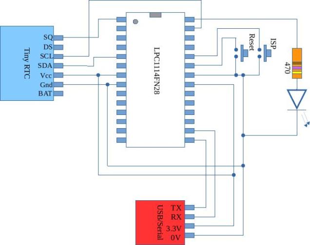
The DS1307 on the Tiny RTC can generate a square wave every second. This can be used as a periodic interrupt to wake the LPC1114 from a deep sleep. GPIO0 pins 0 to 11 and GPIO 1 bit 0 can trigger a wake event; in this case, GPIO0 bit 8 (GPIO0_8) was used. This involves a little bit of interrupt configuration and some confusion as GPIO0_8 can be used as a general purpose external interrupt as well as a wake-up interrupt. These are not programmed in the same way. Anyway, during deep sleep, current consumption drops to 67 micro amps, and runs up to about 12mA during full speed operation. No doubt more tweaking code be done to reduce these figures further. Code is available over here on github
The code contains a function called lp_ports which configures all unused GPIO’s as outputs and turns off pull up resistors. I didn’t find this made much difference so the function remains but is not called.
I bought a TinyRTC module on dx.com for a couple of euro. It contains an at24c32 32k flash memory IC and a ds1307 real time clock IC. The pictures below show how it was interfaced (via I2C) to an LPC1114FN28. The LPC1114 was programmed using ISP/IAP over a USB to serial interface. GCC 5.2.1 was used to compile code and LPC21ISP was used to download it.

Top view of TinyRTC module on breadboard
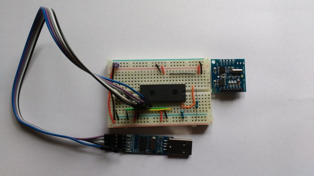
Bottom view of Tiny RTC on breadboard.
The code to drive all of this is available on this github page
The code consists of the following modules:
init : This contains the interrupt vector table and a startup routine which initializes global and static variables, bumps the clock speed up to 48MHz and finally calls on main.
serial : This module manages the UART interface and is used extensively to output run time and debugging information
i2c : This module manages the I2C interface and is implemented as recommended in the LPC1114 reference manual . The I2C interface is implemented as a state machine in hardware and takes a little getting used to. If you enable debugging (uncomment the line #define DEBUG 1 at the start of the i2c.c file) the module outputs debug trace data showing all of the states visited by the I2C state machine.
ds1307: This manages the interface to the RTC and has set/get date routines.
at24c32: This manages the interface with the AT24C32 memory IC and contains functions to read and write random data (be careful of the 1 million write cycles).
main: This is the top level application which exchanges data with the DS1307 and AT24C32.
The DS1307 is capable of outputting a 1Hz square wave which may be used to wake a slumbering MCU from a power saving deep sleep. Hopefully I will get around to this in a future post.
I’ve been struggling with this demonstrator of assembler on the LPC1114 for a while but finally cracked it (on a train ride across the country :). Hope this is instructive to somebody. I think I have stripped the assembler directives down as much as possible, if you find a mistake please comment below.
// Minimal assembler blinky example for LPC1114FN28
// This program flashes an LED on and off.  It is used as a
// demonstrator for class work
// LED is on GPIO0 bit 2
		.syntax unified
		.cpu cortex-m0	// Which variant we are using
		.thumb  /* Cortex micros only understand thumb(2) code	*/
		.global Vector_Table, start
/* Set up interrupt vector table */
		.text
/* It would seem that the LPC1114FN28 treats the area of flash used by
the first 16 vectors as special.  If you attempt to place code here
it doesn't work so you must either skip past this space or just place
dummy values here */
Vector_Table:
	.word     0x10001000 	/* Top of Stack */
    .word     start     	/* Reset Handler */
    .word 	  0		/* NMI */
	.word 	  0		/* Hard Fault */
	.word 	  0     	/* Reserved */
	.word 	  0     	/* Reserved */
	.word 	  0   	    	/* Reserved */
	.word 	  0  	     	/* Reserved */
	.word 	  0   	     	/* Reserved */
	.word 	  0  	      	/* Reserved */
	.word 	  0   	     	/* Reserved */
	.word 	  0		/* SVC */
	.word 	  0    	    	/* Reserved */
	.word 	  0     	/* Reserved */
	.word 	  0 		/* PendSV */
	.word 	  0 		/* SysTick */


/* the program starts here */
	.thumb_func		// The LSB of the address of thumb instructions is
				// required to be 1 - the LSB is used as a flag to
				// indicate thumb instructions are being used.
				// The Cortex M series of processors only understand
				// thumb instructions so if PC is loaded with an
				// address with LSB = 0 then this is treated as an
				// an illegal instruction
				// the .thumb_func directive forces the LSB of
				// 'start' to be 1

start:
// Do initial IO configuration
// Turn on the clocks for GPIO and IOCON
		ldr R1,SYSAHBCLKCTRL	// make pointer to register
		ldr R0,[R1]		// read current value
		ldr R2,SYSAHBCLKMASK	// read desired bit pattern
		orrs R0,R0,R2		// combine with register contents
		str R0,[R1]		// write back to register
// Make sure pin 25 behaves as a GPIO
		ldr R1,IOCON_PIO0_2	// make pointer to register
		ldr R0,[R1]		// read current value
		ldr R2,IOCONMASK	// read desired bit pattern
		bics R0,R0,R2		// combine with register contents
		str R0,[R1]		// write back to register
// Make pin 25 behave as an output
		ldr R1,GPIO0DIR		// make pointer to register
		ldr R0,[R1]		// read current value
		ldr R2,GPIO0MASK	// read desired bit pattern
		orrs R0,R0,R2		// combine with register contents
		str R0,[R1]		// write back to register

// Now enter the main loop
main_loop:
// Set bit 2
		ldr R1,GPIO0DATA	// make pointer to port data register
		ldr R0,[R1]		// read current value
		ldr R2,GPIO0MASK	// read bit pattern
		orrs R0,R0,R2		// set bits
		str R0,[R1]		// write new value

		bl delay		// Leave the LED on for a while

// clear bit 2
		ldr R1,GPIO0DATA	// make pointer to port data register
		ldr R0,[R1]		// read current value
		ldr R2,GPIO0MASK	// read mask
		bics R0,R0,R2		// clear bits
		str R0,[R1]		// write new value

		bl delay		// Leave the LED on for a while

		b	main_loop	/* branch back to start of loop */

delay:	ldr R3,DELAYLENGTH
delay_loop:
		subs R3,R3,#1
		bne delay_loop
		bx LR
// Constants go below here
		.align 2		/* Must force realignment again here */
GPIO0DATA: 	.word 	0x50003ffc
GPIO0DIR: 	.word 	0x50008000
SYSAHBCLKCTRL: 	.word	0x40048080
IOCON_PIO0_2:	.word 	0x4004401c
SYSAHBCLKMASK:	.word   0x10040
IOCONMASK:	.word   0x3
GPIO0MASK:	.word 	0x04
NOTGPIO0MASK:	.word 	0xfffffffb
DELAYLENGTH:	.word 	0xfffff
The Linker script file is as follows:
MEMORY
{
    flash : org = 0x00000000, len = 32k
    ram : org = 0x10000000, len = 4k
}

SECTIONS
{

	. = ORIGIN(flash);
        .text : {
		  *(.vectors); /* The interrupt vectors */
		  *(.text);
        } >flash
	. = ORIGIN(ram);
        .data : {
	  INIT_DATA_VALUES = LOADADDR(.data);
	  INIT_DATA_START = .;
	    *(.data);
	  INIT_DATA_END = .;
        } >ram AT>flash
	BSS_START = .;
	.bss : {

	    *(.bss);

	} > ram
	BSS_END = .;
}
And finally the makefile is
# Specify the compiler to use
CC=arm-none-eabi-gcc
# Specify the assembler to use
AS=arm-none-eabi-as
# Specity the linker to use
LD=arm-none-eabi-ld

CCFLAGS=-mcpu=cortex-m0 -mthumb -g
ASFLAGS=-mcpu=cortex-m0 -mthumb -g --warn
# List the object files involved in this project
OBJS=	blinky.o
blinky.elf : $(OBJS)
	$(LD) $(OBJS) -T linker_script.ld --cref -Map blinky.map -nostartfiles -o main.elf
	 objcopy -O ihex main.elf main.hex
blinky.o: blinky.s
	$(AS) $(ASFLAGS) blinky.s -asghl=blinky.lst -o blinky.o
# if someone types in 'make clean' then remove all object files and executables
# associated wit this project
clean:
	rm $(OBJS)
	rm blinky.elf
I’ve been experimenting with git and github and decided to upload a version of LPC21ISP that is patched for the LPC824 (see an earlier post). It can be found at this link:
ARM have developed a range of optimized DSP functions for all of the Cortex MCU’s. I have found them a challenge to use in “baremetal” gcc based projects as they rely on a particular directory structure and certain compiler directives. The project linked below tackles these difficulties and implements a real-time Finite Impulse Response FIR low pass filter on an STM32F303 Nucleo board. The filter has a sample rate of 20kHz and a cut-off frequency of 1kHz. Initial evaluations indicate the filter performs well and further experimentation will definitely follow.
The output voltage at 500Hz is shown in yellow below (input signal is green trace).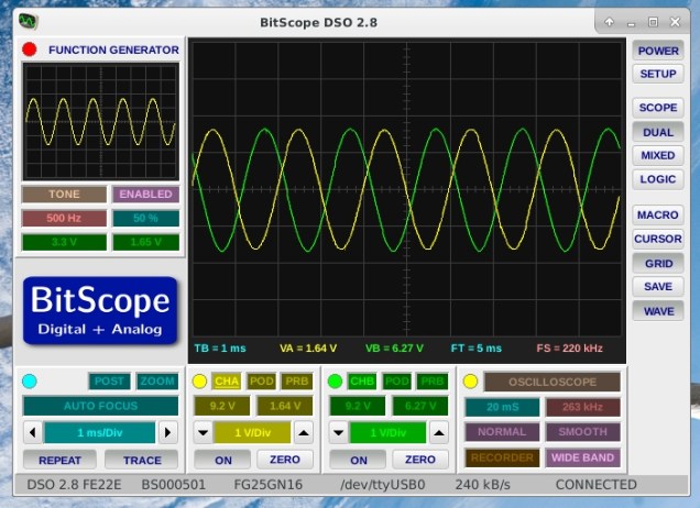
The output voltage at 1kHz is shown in yellow below. The roll off is a little more than expected but this could be the result of truncating of coefficients.

Code and further explanatory documentation is available here:
http://eleceng.dit.ie/frank/arm/BareMetalSTM32F303Nucleo/fir/
Two new examples for the stm32f303 nucleo board are available for download. The first of these outputs ADC conversion results over the serial port (serialadc). The second performs a simple analog pass-through function sending the ADC output to the DAC. Sample rates over 100kHz are possible. This example uses the systick interrupt to generate a reliable sample rate. More details here:
http://eleceng.dit.ie/frank/arm/BareMetalSTM32F303Nucleo/index.html
