Waiting for /CS

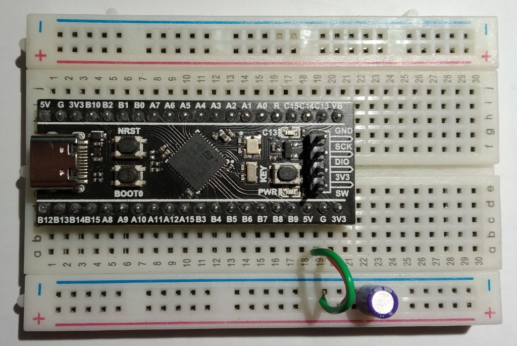
I have been working on an interface between an STM32G431 and a W25Q128FV SPI flash memory chip (128 Mbit/16MByte). The image above shows the memory chip on a breakout board with a surface mount capacitor next to it. Given the nature of breadboards and the wires used I’ve been running the memory interface at a reduced speed (1.3MHz). A PCB will be used at a later stage and which should allow for higher speeds.

Erasing the chip was presenting some problems. The code for erase was as follows:

void serial_flash::bulk_erase()
{
	write_enable();
	SPI->startTransaction();
	SPI->transfer((uint8_t)0xc7);	
	SPI->stopTransaction();
	while(read_status1() & 1); // wait until erase has completed
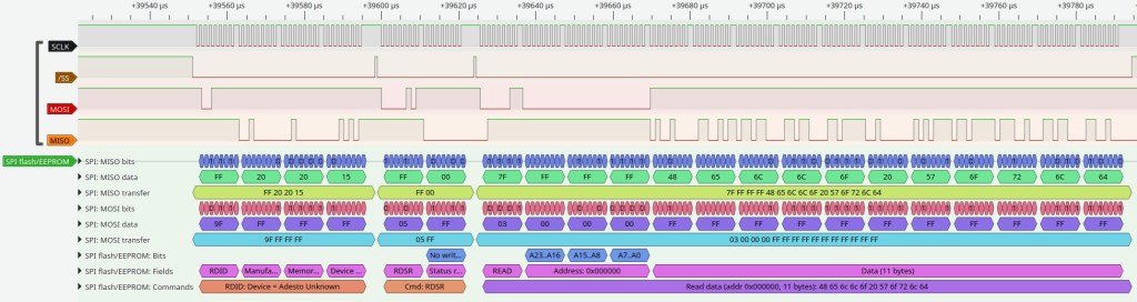
}

The chip must be put into “write” mode before the erase command (0xC7) is sent. The function exits when the “busy” bit in status register 1 is clear. While everything seemed ok, the function did not erase the chip. I took a closer look at the SPI bus using a logic analyzer. I have a very cheap logic analyzer which doesn’t have a very good trigger mechanism. My normal workaround for this is to put the area under test into an everlasting loop and then view the pins of interest on the logic analyzer. This is a problem for erase operations like this as the SPI flash chip has only so many erase cycles. As a precaution I change the command code to 0xd7 (not a supported command) which allowed me look at the SPI bus without harming the chip. I also commented out loop that polled the status register.

The write enable command (0x06) is plainly visible as is the “fake” chip erase command 0xd7. The CS line is driven low just before the 0x06 command and goes high some time after the 0xd7 command. This is not the correct way to erase this chip. The data sheet clearly states that the CS line must go high for a period after each command. It does not do this after the write enable command. The write_enable function is as follows:

void serial_flash::write_enable(void)
{
	SPI->startTransaction();
	SPI->transfer((uint8_t)0x06);	
	SPI->stopTransaction();		
}	

The stopTransaction function should drive the CS line high but it didn’t seem to be working. The relevant SPI code is:

void spi::stopTransaction(void)
{	
	volatile unsigned Timeout = 1000;    
	while (SPI1->SR & ((1 << 12) + (1 << 11)) );     // wait for fifo to empty
	while (((SPI1->SR & (1 << 0))!=0)&&(Timeout--)); // Wait for RXNE
	Timeout = 1000;    
	while (((SPI1->SR & (1 << 1))==0)&&(Timeout--)); // Wait for TXE
	Timeout = 1000;    
	while (((SPI1->SR & (1 << 7))!=0)&&(Timeout--)); // Wait for Busy		
	SPI1->CR1 &= ~(1 << 6); // Disable SPI (SPE = 0)
				
}

This should have worked but it clearly didn’t. Thinking about the sequence of events involved in the bulk_erase function it occurred to me that the call to startTransaction just after the write_enable command may actually be happening before the SPI peripheral had a chance to raise the CS line. The SPI peripheral is routed through GPIO port A in this setup. I noticed that I could monitor the status of the CS pin by reading GPIOA’s input data register and hence wait for it to go high. The stopTransaction code was modified as follows:

void spi::stopTransaction(void)
{	
	volatile unsigned Timeout = 1000;    
	while (SPI1->SR & ((1 << 12) + (1 << 11)) );     // wait for fifo to empty
	while (((SPI1->SR & (1 << 0))!=0)&&(Timeout--)); // Wait for RXNE
	Timeout = 1000;    
	while (((SPI1->SR & (1 << 1))==0)&&(Timeout--)); // Wait for TXE
	Timeout = 1000;    
	while (((SPI1->SR & (1 << 7))!=0)&&(Timeout--)); // Wait for Busy		
	SPI1->CR1 &= ~(1 << 6); // Disable SPI (SPE = 0)
		
	while((GPIOA->IDR & (1 << 4))==0); // wait for CS to go high
	
}

This produced the following output from the logic analyzer:

A high pulse can now be seen between the two SPI commands. As a final test, I replaced the fake “0xD7” command with “0xC7” and presto: erases now work.

The STM32F411 “Black Pill”

The STM32F411 “Black Pill” board is a step up in performance from the Blue Pill (STM32F103). It contains a 100MHz ARM Cortex M4F CPU with 512kB Flash and 128kB of RAM. The usual sort of peripherals are also included (ADC, Timers, SPI, I2C etc.).

The Black Pill board comes with a set of pads on the underside that can accommodate an SPI flash chip. I was interested in giving this a go so soldered in an ST Micro M25P16 device. This has 2MB of storage that is page programmable (256 Byte pages) and sector erasable (64kB sector size). It also supports a bulk erase function.

There were no great problems getting a driver going except for one thing: When NSS is released (sent high) by the SPI peripheral I found that I had to introduce a short delay in the SPI driver. Without this delay, the interface to the flash chip did not work when one transaction immediately followed another. This may be because the pulse never left the STM32F411, or because of bad wiring, or because the flash chip just needs a moment (the datasheet seems to suggest at lease 100ns of a pause). Anyway, it now works and the image below shows a data read transaction captured using pulseview (Thanks pulseview authors! 🙂 ).

You can just make out the narrow NSS pulses (approx 400ns) that were necessary for the system to work. This image was captured with the SPI bus running at a reduced speed to allow for the limited bandwidth of my logic analyzer.

What could this be used for? Well, a data logger perhaps, or a store for various image assets for a screen or maybe even some sounds. If you use this be mindful of the write cycle limitation of these devices and especially don’t put a write in a fast loop.

Code for this and other examples can be found over on github : https://github.com/fduignan/stm32f411

STM32L031 controlling a PL9823 LED using SPI

stm32l031_pl9823
The PL9823 is a smart LED much like the WS2812B. There are some slight timing differences and they can sometimes be found cheaper than an equivalent WS2812B. I got hold of a few from Aliexpress in a frosted 8mm package with 4 pins that allow them to be used in a breadboard.
In a previous post I outlined how SPI could be used with an STM32F042 to drive a WS2182b. Things were a little different in this case as the STM32L031 has fewer options with the SPI clock and the slightly different timing requirements of the PL9823. pl9823_mosi
The image above shows the control from the MOSI signal for a nearly white colour on the LED. The signal is shows a 12 byte sequence which is interpreted as a 3 byte RGB sequence by the PL9823. A PL9823 logic ‘1’ is sent by sending 3 SPI ‘1’s followed by a zero. This takes 2 microseconds. A logic ‘0’ is sent by sending a single SPI ‘1’ and 3 SPI ‘0’s. The sequence is generated using the following function

void writePL9823(uint32_t Colour)
{
    // each colour bit should map to 4 SPI bits.
    // Format of Colour (bytes) 00RRGGBB
    uint8_t SPI_Output[12];
    int SrcIndex = 0;
    int DestIndex = 0;
    for (DestIndex = 0; DestIndex < 12; DestIndex++)
    {
        if (Colour & (1 << 23))
        {
            SPI_Output[DestIndex] = 0xe0;
        }
        else
        {
            SPI_Output[DestIndex] = 0x80;
        }
        Colour = Colour << 1;
        if (Colour & (1 << 23))
        {
            SPI_Output[DestIndex] |= 0xe;
        }
        else
        {
            SPI_Output[DestIndex] |= 0x8;
        }
        Colour = Colour << 1;
    }
    for (int i=0;i<12;i++)
    {
        transferSPI(SPI_Output[i]);
    }
}

The code expands a 3 byte colour sequence into a 12 byte one and sends it over an SPI link running at 2MHz. This is sufficient to match the timing requirements of the PL9823.
A demo program which cycles through various colours can be found over on github.

Using an SPI Flash chip with the STM32L031 Nucleo and mbed

breadboard_spi_flash_stm32l031

The W25Q32 is a 4 MByte SPI Flash ROM device which costs about 30 cents. It comes in an 8 pin surface mount package and so must be mounted on a breakout board if you want to use it with a breadboard. I designed a breakout board with KiCad and you can see it in the above image.

A test program was written along with a C++ class to encapsulate the device’s functions. The test program begins by powering up the device, it then does a bulk erase followed by a write of the string “Hello World”. The main loop then continuously reads this string back from the chip. Be careful how often you erase the device – you only get so many write/erase cycles.
This sort of device could be useful for event logging in an embedded system or it could be used to store an large program that is pulled in to RAM by a bootloader.

file: main.cpp

// Developed on the NUCLEO-L031K6 board from ST Micro and 
// the W25Q32BV SPI Flash rom
#include "mbed.h"
#include "spiflash.h"
DigitalOut myled(LED1);
SPI spi(PB_5, PB_4, PB_3);
Serial pc(USBTX, USBRX);
DigitalOut nSS(PA_11);
spiflash Myflash(spi,nSS);

int main() {     
    spi.format(8,3);  
    pc.printf("Powering up\r\n");
    Myflash.powerUp();   
    wait(0.1);
    pc.printf("Erasing\r\n");
    Myflash.eraseAll();    
    pc.printf("Writing\r\n");    
    Myflash.writeDataBytes(0,(uint8_t *)"Hello World",11);    
    while(1) {
        uint8_t Contents[16];                
        // Write guard bytes to the end of the buffer to test operation
        // of read function.
        Contents[13]=13;
        Contents[14]=14;
        Contents[15]=15;        
        Myflash.readDataBytes(0,Contents,14);
        pc.printf("\r\n++++++++++++++++++++++++++++++++++\r\n");
        for (int i=0;i < 16; i++)
        {
            pc.printf("%02x ", Contents[i]);
        }             
        myled = 1; // LED is ON
        wait(0.2); // 200 ms
        myled = 0; // LED is OFF
        wait(1.0); // 1 sec
        pc.printf("\r\nID = %X\r\n",Myflash.readDeviceIdentifier());
    }
}

The listings for the spiflash class are listed further down this post. I used PulseView and a cheap 8 channel USB logic analyzer to capture the following waveforms for the function readDeviceIdentifier()
pulseview_spi_flash_stm32l031

file: spiflash.h

#ifndef __spiflash_h
#define __spiflash_h
#include "mbed.h"
class spiflash {
public:
    spiflash(SPI &Spi, DigitalOut & NSS);
    void powerUp();
    void eraseAll();
    void eraseSector(uint32_t Address);
    void enableWrite();
    void disableWrite();
    void readDataBytes(uint32_t Address, uint8_t *ByteArray, uint32_t Length);
    void writeDataBytes(uint32_t Address, uint8_t *ByteArray, uint32_t Length);
    uint32_t readDeviceIdentifier();

private:
    static const uint32_t FlashMemorySize=4194304; // Capacity of W25Q32BV
    static const uint32_t SectorSize=4096; // Erase sector size
    static const uint32_t PageSize=256; // Number of bytes that can be programmed at one time
    SPI & spi;
    DigitalOut &nSS;    
    uint32_t readStatusRegister1();
};
#endif

file: spiflash.cpp

#include "spiflash.h"
spiflash::spiflash(SPI &Spi, DigitalOut & NSS) : spi(Spi), nSS(NSS)
{
   
}
void spiflash::powerUp()
{
    char TxBuffer[4];  // Transmit buffer
    char RxBuffer[4];  // Receive buffer
    TxBuffer[0]=0xAB;  // Command 0xAB = "Release from power down"
    nSS = 0;           // Drive nCS low to connect slave to the bus
    spi.write(TxBuffer,1,RxBuffer,1); // Write 1 byte and read 1 byte
    nSS = 1;           // Drive nCS high to disconnect slave from the bus
}
void spiflash::eraseAll()
{
    enableWrite();
    // Use sparingly!!! Limited number of cycles available
    char TxBuffer[4];  // Transmit buffer
    char RxBuffer[4];  // Receive buffer
    TxBuffer[0]=0xc7;  // Command 0xc7 = "Bulk Erase"
    nSS = 0;           // Drive nCS low to connect slave to the bus
    spi.write(TxBuffer,1,RxBuffer,1); // Write 1 byte and read 1 byte
    nSS = 1;           // Drive nCS high to disconnect slave from the bus
    while (readStatusRegister1() & 1)
    { // Wait for device erase to complete       
    }
}
void spiflash::eraseSector(uint32_t Address)
{
    enableWrite();
    // Mask off the lower bits of the Sector Address (redundant?)
    //Address = Address & 0xfffc00; //0b1111 1111 1111 1100 0000 0000
    // Use sparingly!!! Limited number of cycles available
    char TxBuffer[4];  // Transmit buffer
    char RxBuffer[4];  // Receive buffer
    
    TxBuffer[0]=0x20;  // Command 0x20 = "Sector Erase"
    TxBuffer[1] = (Address >> 16) & 0xff;
    TxBuffer[2] = (Address >> 8) & 0xff;
    TxBuffer[3] = (Address & 0xff);
    nSS = 0;           // Drive nCS low to connect slave to the bus
    spi.write(TxBuffer,4,RxBuffer,1); // Write 1 byte and read 1 byte
    nSS = 1;           // Drive nCS high to disconnect slave from the bus
    while (readStatusRegister1() & 1)
    {
        // Wait for sector erase to complete
    }
}
void spiflash::enableWrite()
{
    char TxBuffer[4];  // Transmit buffer
    char RxBuffer[4];  // Receive buffer
    TxBuffer[0]=0x06;  // Command 0x06 = "Enable writes"
    nSS = 0;           // Drive nCS low to connect slave to the bus
    spi.write(TxBuffer,1,RxBuffer,1); // Write 1 byte and read 1 byte
    nSS = 1;           // Drive nSS high to disconnect slave from the bus
}
void spiflash::disableWrite()
{
    char TxBuffer[4];  // Transmit buffer
    char RxBuffer[4];  // Receive buffer
    TxBuffer[0]=0x06;  // Command 0x06 = "Disable writes"
    nSS = 0;           // Drive nCS low to connect slave to the bus
    spi.write(TxBuffer,1,RxBuffer,1); // Write 1 byte and read 1 byte
    nSS = 1;           // Drive nSS high to disconnect slave from the bus
}
void spiflash::readDataBytes(uint32_t Address, uint8_t *ByteArray, uint32_t Length)
{    
    // Read Length bytes starting at Address and return in ByteArray
    char TxBuffer[4];   // Transmit buffer
    TxBuffer[0]=0x03;   // Command 0x03 = "Read bytes"
    nSS = 0;
    TxBuffer[1] = (Address >> 16) & 0xff;
    TxBuffer[2] = (Address >> 8) & 0xff;
    TxBuffer[3] = (Address) & 0xff;
    spi.write(TxBuffer,4,0,0); // Send command and Address of interest
    spi.write(0,0,(char *)ByteArray,Length); // Send command and Address of interest
    nSS = 1;
}
void spiflash::writeDataBytes(uint32_t Address, uint8_t *ByteArray, uint32_t Length)
{
    enableWrite();
    char TxBuffer[4];   // Transmit buffer
    
    TxBuffer[0]=0x02;   // Command 0x02 = "Write bytes"
    TxBuffer[1] = (Address >> 16) & 0xff;
    TxBuffer[2] = (Address >> 8) & 0xff;
    TxBuffer[3] = (Address) & 0xff;
    nSS = 0;
    spi.write(TxBuffer,4,0,0); // Send command and Address of interest
    spi.write((char *)ByteArray, Length, 0,0); // Send command and Address of interest
    nSS = 1;
    while (readStatusRegister1() & 1)
    {
        // Wait for write data to complete
    }
}
uint32_t spiflash::readDeviceIdentifier()
{
    // If the chip conforms with JEDEC norms, the last byte of the ID should 
    // indicate the capacity.  The last byte is the size of the chip express
    // in powers of 2.  For example if you read 0x16 (22 decimal) then the
    // chip should have a capacity of 2^22 = 4MiB.
    char TxBuffer[4];  // Transmit buffer
    char RxBuffer[4];  // Receive buffer
    TxBuffer[0]=0x9f;  // Command 0x9f = "Read status Device ID"
    nSS = 0;           // Drive nCS low to connect slave to the bus
    spi.write(TxBuffer,1,RxBuffer,4); // Write 1 byte and read 4 bytes
    nSS = 1;           // Drive nCS high to disconnect slave from the bus
    uint32_t ID=RxBuffer[1];
    ID = ID << 8;
    ID += RxBuffer[2];
    ID = ID << 8;
    ID += RxBuffer[3];
    return ID; // return the status register contents     
}
uint32_t spiflash::readStatusRegister1()
{
    char TxBuffer[4];  // Transmit buffer
    char RxBuffer[4];  // Receive buffer
    TxBuffer[0]=0x05;  // Command 0x9f = "Read Status register 1"
    nSS = 0;           // Drive nCS low to connect slave to the bus
    spi.write(TxBuffer,1,RxBuffer,2); // Write 1 byte and read 1 byte
    nSS = 1;           // Drive nCS high to disconnect slave from the bus
    return RxBuffer[1]; // return the status register contents 
    
}

Interactive SPI

The SPI protocol can be tricky enough to get working especially if you are unsure of the MCU you are using and/or the peripheral.  Logic analyzers can help but can also be expensive.  With the help of the following Energia MSP430G2553 code and a dumb terminal serial application program (on your PC) you can interact live with an SPI peripheral and hopefully come to grips with its operation.

The peripheral can be wired as follows:
LaunchPads-MSP430G2-—-Pins-Maps-13-42

Launchpad                   Peripheral
MOSI------------------------MOSI
MISO------------------------MISO
P1_0------------------------SS (slave select or CE)
GND-------------------------GND
Vcc-------------------------Vcc

Check the peripheral power requirements first and don’t connect a 5V peripheral directly to a 3.3V MSP430

The program presents the user with a simple menu:

Please select from one of the following:
0: SS Low
1: SS High
2: Write byte
3: Read byte

If you choose 0 or 1, SS is raised or lowered as appropriate and the menu recycles. If you choose 2 you see this (I entered the value ‘a9’ (not case sensitive))

Please select from one of the following:
0: SS Low
1: SS High
2: Write byte
3: Read byte
Enter a 2 character hex value: a9
Out : A9
In : 0

If you choose 3 you will see something like this:

Please select from one of the following:
0: SS Low
1: SS High
2: Write byte
3: Read byte
In : 0

The code is shown below. You will probably need to check out which SPI modes and byte ordering suit you. Also, the SPI interface is running at the very low speed of 125kHz. This was deliberate as it reduces the risk of data errors on shaky test leads and may help debugging. You can of course change this. The divider is divided into 16MHz to give an SPI data rate. This is very definitely version 0.1 and changes are likely in the future when I do some real testing.

/*
 * SPI protocol tester using the MSP430G2553 G2 Launchpad
 * This program allows you manage an SPI bus,write and read data
 * using a serial dumb terminal application
 * The program makes use of the Energia Serial and SPI libraries
 * Serial interface : 9600,n,8,1
 * SPI library reference : http://energia.nu/reference/spi/
 * 
 */
#include <SPI.h>

// Will use P1_0 as SS pin as there is a handy LED there on the launchpad
#define SS_Pin  P1_0


int getUserCommand();
int getInteger(String Prompt);
void setup() {
  // put your setup code here, to run once:
  // Default SPI configuration : feel free to change!
  // Set up the SS Pin and make it HIGH initially (low wakes up a slave)
  pinMode(SS_Pin,OUTPUT);  
  digitalWrite(SS_Pin,HIGH);
  SPI.begin();
  SPI.setDataMode(SPI_MODE0); // can choose modes 0,1,2,3
  SPI.setBitOrder(MSBFIRST);  // can be MSBFIRST or LSBFIRST
  SPI.setClockDivider(128);   // assuming a system clock of 16MHz this gives an 
                              // SPI speed of 125kHz - deliberately slow to be more forgiving and
                              // to make signals easier to see with a scope of logic analyser
  // Serial communications to host setup
  Serial.begin(9600);
}
int TXByte,RXByte;
void loop() {
  
  // put your main code here, to run repeatedly: 
  switch (getUserCommand())
  {
    case 0 : {
      // Command 0 : drop SS pin down
      digitalWrite(SS_Pin,LOW);    
      break;
    }
    case 1 : {
      // Command 1 : raise SS pin up
      digitalWrite(SS_Pin,HIGH);
      break;
    }
    case 2 : {
      // Command 2 : send a byte
      TXByte = getInteger("Enter a value to transmit: ");
      RXByte = SPI.transfer(TXByte);
      Serial.print("Out : ");
      Serial.println(TXByte,HEX);
      Serial.print("In : ");
      Serial.println(RXByte,HEX);
      break;
    }
    case 3 : {
      // Command 3 : read a byte (send a dummy byte out)
      RXByte = SPI.transfer(0x00);
      Serial.print("In : ");
      Serial.println(RXByte,HEX);
      break;      
    }
    default : {
      Serial.println("Invalid choice");
    }
  }
  delay(100);
}
int showMenu(String Menu[],int MenuItemCount)
{
  Serial.flush();
  Serial.println("Please select from one of the following:");
  for (int item=0; item < MenuItemCount; item++)
  {
    Serial.print(item);
    Serial.print(": ");
    Serial.println(Menu[item]);
  }
  while(Serial.available()==0);
    
  return Serial.read() - '0'; // assuming a numeric choice is made - convert to decimal from ascii
}

int getUserCommand()
{
  String Menu[4];
  Menu[0]="SS Low";
  Menu[1]="SS High";
  Menu[2]="Write byte";
  Menu[3]="Read byte";
  return showMenu(Menu,4);
  
}
int HexDigitToDecimal(char Digit)
{
  if ( (Digit >= '0') && (Digit <= '9') )
  {
    return Digit - '0';
  }
  Digit = Digit | 32; // enforce lower case
  if ( (Digit >= 'a') && (Digit <= 'f') )
  {
    return Digit - 'a' + 10;
  }
  return 0;
}
int getInteger(String Prompt)
{
  char HexString[3];
  int ReturnValue = 0;
  HexString[2]=0;
  Serial.flush();
  Serial.print("Enter a 2 character hex value: ");
  while(Serial.available()==0);  
  HexString[0]=Serial.read();Serial.print(HexString[0]);
  while(Serial.available()==0);  
  HexString[1]=Serial.read();Serial.println(HexString[1]);
  ReturnValue = HexDigitToDecimal(HexString[0]);
  ReturnValue = ReturnValue << 4;
  ReturnValue += HexDigitToDecimal(HexString[1]);
  return ReturnValue;
}


9 DOF on the STM32L476 Discovery board

The STM32L476 Discovery board has an LSM303 Accelerometer/Compass IC and an L3GD20 gyroscope attached to the MCU using an SPI bus and some chip select lines.  I wanted to experiment with them with a view to putting together a balancing robot.  Supporting code for the following was needed for this:

  • an SPI interface
  • the LSM303
  • the L3GD20
  • serial communications
  • periodic interrupts to pace data capture

Rather than build a complex Makefile I went with a simple shell script (or batch file if you prefer) with the following commands:

arm-none-eabi-gcc -static -mthumb -g -mcpu=cortex-m4 *.c -T linker_script.ld -o main.elf -nostartfiles
arm-none-eabi-objcopy -g -O binary main.elf main.bin

Note: your PATH environment variable must include the directory where arm-none-eabi-gcc is located.

The resulting main.bin file can then be copied to the virtual disk presented by the mbed interface on the STM32L476 discovery board.  (The program waits for you to press the centre joystick button before starting).`

Serial communications is carried out over the built-in ST-Link USB-Serial emulator so no additional hardware is needed (9600,n,8,1).

Code is available over here