Multi-threading on the STM32L031 Nucleo with the Keil IDE

An earlier blog post showed multi-threading on the TI MSP432. Recently I have been working on an STM32L031 Nucleo board with the Keil ARM-MDK environment. I wanted to demonstrate multi-threading and so ported the code from the MSP432 to the L031. A section of the main.c file looks like this:


#define STACK_SIZE 128
__attribute__((noreturn))  void threadA(void);
__attribute__((noreturn)) void threadB(void);
__attribute__((noreturn)) void threadC(void);
static uint32_t StackA[STACK_SIZE];
static uint32_t StackB[STACK_SIZE];
static uint32_t StackC[STACK_SIZE];

void threadA()
{
	while (1)
	{
		static int State = 0;
		if (State == 0)
		{
			GPIOA->ODR &=~(1u << 0);
			State = 1;
		}
		else
		{
			GPIOA->ODR |= (1 << 0);
			State = 0;
		}
		delay(100000);
	}	
}
int main()
{
	// Initialize I/O ports
	RCC->IOPENR = 1; // Enable GPIOA
	pinMode(GPIOA,0,1); // Make GPIOA Bit 0 an output
	pinMode(GPIOA,1,1); // Make GPIOA Bit 1 an output
	pinMode(GPIOA,2,1); // Make GPIOA Bit 2 an output
	initClock();		// Set the MCU running at 16MHz
	createThread(threadA,StackA, STACK_SIZE);
	createThread(threadB,StackB, STACK_SIZE);
	createThread(threadC,StackC, STACK_SIZE);
	startSwitcher();
}

Three threads are created in this example and they each change the state of a bit on Port A. I should have used the BSRR register to set and clear the bits but for the purposes of getting the ideas behind multi-threading across this was sufficient. The createThread function takes three arguments: The thread’s start address, a pointer to the thread’s stack and the size of this stack. Stacks for the threads are simply declared as arrays of uint32_t’s.

The startSwitcher function starts the SysTick timer running, does some stack adjustments and enables interrupts. It does not return. The SysTick handler is written in assembler and it performs the context switch between threads.

Source code is available on github. I did not include the project (uvproj) files as they contain lots of path information that would not transfer to other systems. If you want to try this for yourself just create a project for the STM32L031 Nucleo in Keil and add the files from github. You should first remove the other source files in your project.

Using the TLS2561 to wake the STM32L031 from sleep

stm32l031_ssd1306_tls2561_circuit
In some ways this example is a bit illogical. The TLS2561 consumes a few hundred micro amps while operating so using it to wake the STM32L031 from sleep doesn’t make a lot of sense. This example may be relevant to those who want to use an external I/O pin to wake the an STM32L031 generally or maybe as part of a larger circuit.

The TLS2561 can generate an interrupt signal when the light received on Channel 0 goes outside a user specified certain range. In this example, the range was arbitrarily set to go from 0 0x100. If the received light is equal to or greater than 0x100 then the interrupt signal is driven low which wakes the MCU. If the light is less than or equal to 0 an interrupt is also generated. This isn’t exactly what I wanted (I only wanted an interrupt if the light was bright) so if the circuit is plunged into complete darkness an interrupt will also be generated. This unintended waking could be dealt with by checking the value on Channel 0 and, if zero, going back to sleep again.

Code is available as usual over on github.

Using the TLS2561 with the STM32L031

stm32l031_tls2561
The TLS2561 is a digital light sensor which senses light on two wavelengths and outputs two 16 bit results. These values are accessed over an I2C bus. This test program simply reads and displays the ADC results. The manufacturer provides a C source example that can then be used to convert this to LUX. For now I’m not particularly interested in this feature. What is possibly of more interest is the interrupt capability of the device which may allow it to wake a slumbering MCU when light levels fall between certain values. This may be of use in a power saving context. More to follow but for now, source code for my various STM32L031 examples can be found over here on github

STM32L031 controlling a PL9823 LED using SPI

stm32l031_pl9823
The PL9823 is a smart LED much like the WS2812B. There are some slight timing differences and they can sometimes be found cheaper than an equivalent WS2812B. I got hold of a few from Aliexpress in a frosted 8mm package with 4 pins that allow them to be used in a breadboard.
In a previous post I outlined how SPI could be used with an STM32F042 to drive a WS2182b. Things were a little different in this case as the STM32L031 has fewer options with the SPI clock and the slightly different timing requirements of the PL9823. pl9823_mosi
The image above shows the control from the MOSI signal for a nearly white colour on the LED. The signal is shows a 12 byte sequence which is interpreted as a 3 byte RGB sequence by the PL9823. A PL9823 logic ‘1’ is sent by sending 3 SPI ‘1’s followed by a zero. This takes 2 microseconds. A logic ‘0’ is sent by sending a single SPI ‘1’ and 3 SPI ‘0’s. The sequence is generated using the following function

void writePL9823(uint32_t Colour)
{
    // each colour bit should map to 4 SPI bits.
    // Format of Colour (bytes) 00RRGGBB
    uint8_t SPI_Output[12];
    int SrcIndex = 0;
    int DestIndex = 0;
    for (DestIndex = 0; DestIndex < 12; DestIndex++)
    {
        if (Colour & (1 << 23))
        {
            SPI_Output[DestIndex] = 0xe0;
        }
        else
        {
            SPI_Output[DestIndex] = 0x80;
        }
        Colour = Colour << 1;
        if (Colour & (1 << 23))
        {
            SPI_Output[DestIndex] |= 0xe;
        }
        else
        {
            SPI_Output[DestIndex] |= 0x8;
        }
        Colour = Colour << 1;
    }
    for (int i=0;i<12;i++)
    {
        transferSPI(SPI_Output[i]);
    }
}

The code expands a 3 byte colour sequence into a 12 byte one and sends it over an SPI link running at 2MHz. This is sufficient to match the timing requirements of the PL9823.
A demo program which cycles through various colours can be found over on github.

Using an SPI Flash chip with the STM32L031 Nucleo and mbed

breadboard_spi_flash_stm32l031

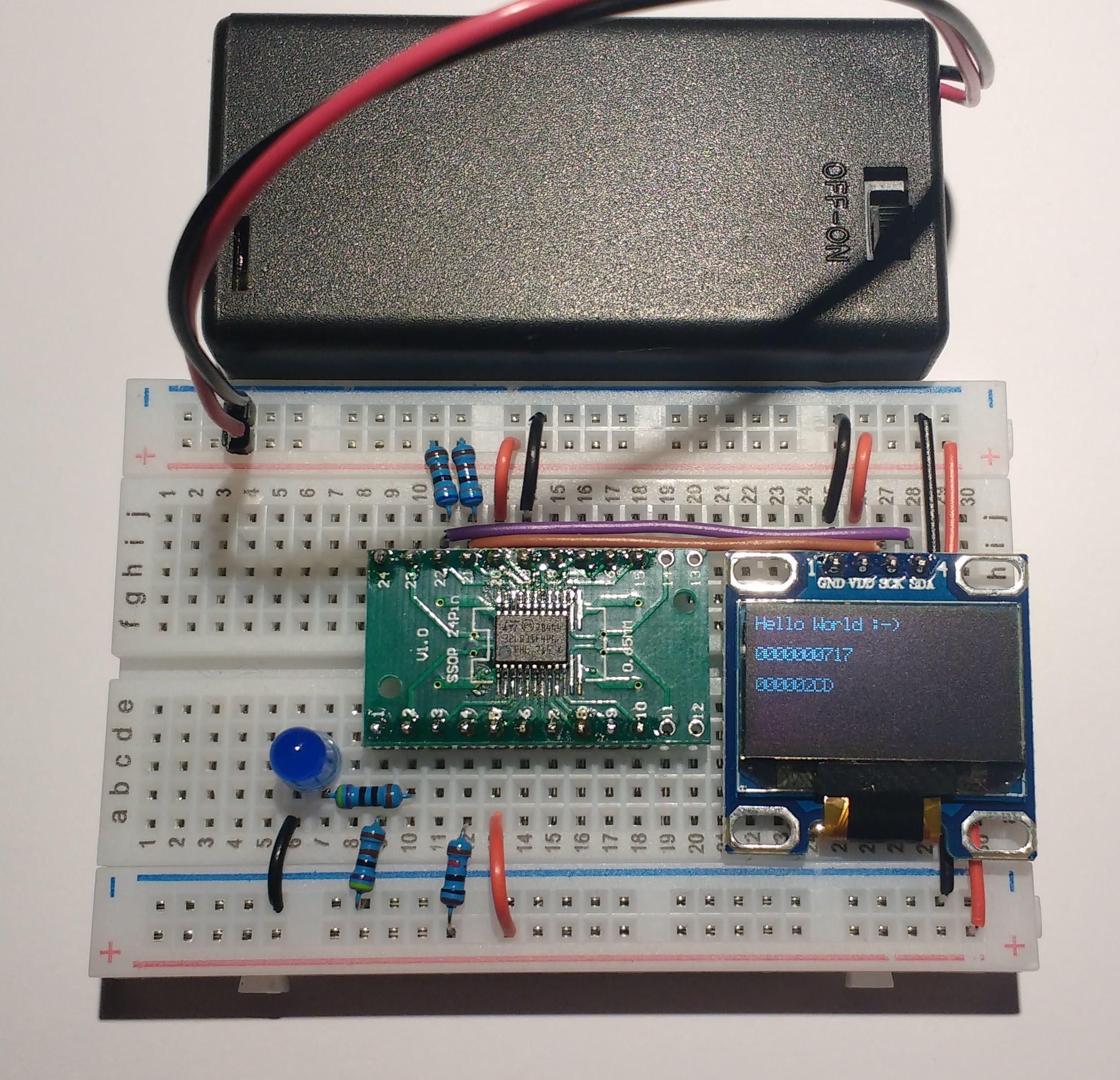
The W25Q32 is a 4 MByte SPI Flash ROM device which costs about 30 cents. It comes in an 8 pin surface mount package and so must be mounted on a breakout board if you want to use it with a breadboard. I designed a breakout board with KiCad and you can see it in the above image.

A test program was written along with a C++ class to encapsulate the device’s functions. The test program begins by powering up the device, it then does a bulk erase followed by a write of the string “Hello World”. The main loop then continuously reads this string back from the chip. Be careful how often you erase the device – you only get so many write/erase cycles.
This sort of device could be useful for event logging in an embedded system or it could be used to store an large program that is pulled in to RAM by a bootloader.

file: main.cpp

// Developed on the NUCLEO-L031K6 board from ST Micro and 
// the W25Q32BV SPI Flash rom
#include "mbed.h"
#include "spiflash.h"
DigitalOut myled(LED1);
SPI spi(PB_5, PB_4, PB_3);
Serial pc(USBTX, USBRX);
DigitalOut nSS(PA_11);
spiflash Myflash(spi,nSS);

int main() {     
    spi.format(8,3);  
    pc.printf("Powering up\r\n");
    Myflash.powerUp();   
    wait(0.1);
    pc.printf("Erasing\r\n");
    Myflash.eraseAll();    
    pc.printf("Writing\r\n");    
    Myflash.writeDataBytes(0,(uint8_t *)"Hello World",11);    
    while(1) {
        uint8_t Contents[16];                
        // Write guard bytes to the end of the buffer to test operation
        // of read function.
        Contents[13]=13;
        Contents[14]=14;
        Contents[15]=15;        
        Myflash.readDataBytes(0,Contents,14);
        pc.printf("\r\n++++++++++++++++++++++++++++++++++\r\n");
        for (int i=0;i < 16; i++)
        {
            pc.printf("%02x ", Contents[i]);
        }             
        myled = 1; // LED is ON
        wait(0.2); // 200 ms
        myled = 0; // LED is OFF
        wait(1.0); // 1 sec
        pc.printf("\r\nID = %X\r\n",Myflash.readDeviceIdentifier());
    }
}

The listings for the spiflash class are listed further down this post. I used PulseView and a cheap 8 channel USB logic analyzer to capture the following waveforms for the function readDeviceIdentifier()
pulseview_spi_flash_stm32l031

file: spiflash.h

#ifndef __spiflash_h
#define __spiflash_h
#include "mbed.h"
class spiflash {
public:
    spiflash(SPI &Spi, DigitalOut & NSS);
    void powerUp();
    void eraseAll();
    void eraseSector(uint32_t Address);
    void enableWrite();
    void disableWrite();
    void readDataBytes(uint32_t Address, uint8_t *ByteArray, uint32_t Length);
    void writeDataBytes(uint32_t Address, uint8_t *ByteArray, uint32_t Length);
    uint32_t readDeviceIdentifier();

private:
    static const uint32_t FlashMemorySize=4194304; // Capacity of W25Q32BV
    static const uint32_t SectorSize=4096; // Erase sector size
    static const uint32_t PageSize=256; // Number of bytes that can be programmed at one time
    SPI & spi;
    DigitalOut &nSS;    
    uint32_t readStatusRegister1();
};
#endif

file: spiflash.cpp

#include "spiflash.h"
spiflash::spiflash(SPI &Spi, DigitalOut & NSS) : spi(Spi), nSS(NSS)
{
   
}
void spiflash::powerUp()
{
    char TxBuffer[4];  // Transmit buffer
    char RxBuffer[4];  // Receive buffer
    TxBuffer[0]=0xAB;  // Command 0xAB = "Release from power down"
    nSS = 0;           // Drive nCS low to connect slave to the bus
    spi.write(TxBuffer,1,RxBuffer,1); // Write 1 byte and read 1 byte
    nSS = 1;           // Drive nCS high to disconnect slave from the bus
}
void spiflash::eraseAll()
{
    enableWrite();
    // Use sparingly!!! Limited number of cycles available
    char TxBuffer[4];  // Transmit buffer
    char RxBuffer[4];  // Receive buffer
    TxBuffer[0]=0xc7;  // Command 0xc7 = "Bulk Erase"
    nSS = 0;           // Drive nCS low to connect slave to the bus
    spi.write(TxBuffer,1,RxBuffer,1); // Write 1 byte and read 1 byte
    nSS = 1;           // Drive nCS high to disconnect slave from the bus
    while (readStatusRegister1() & 1)
    { // Wait for device erase to complete       
    }
}
void spiflash::eraseSector(uint32_t Address)
{
    enableWrite();
    // Mask off the lower bits of the Sector Address (redundant?)
    //Address = Address & 0xfffc00; //0b1111 1111 1111 1100 0000 0000
    // Use sparingly!!! Limited number of cycles available
    char TxBuffer[4];  // Transmit buffer
    char RxBuffer[4];  // Receive buffer
    
    TxBuffer[0]=0x20;  // Command 0x20 = "Sector Erase"
    TxBuffer[1] = (Address >> 16) & 0xff;
    TxBuffer[2] = (Address >> 8) & 0xff;
    TxBuffer[3] = (Address & 0xff);
    nSS = 0;           // Drive nCS low to connect slave to the bus
    spi.write(TxBuffer,4,RxBuffer,1); // Write 1 byte and read 1 byte
    nSS = 1;           // Drive nCS high to disconnect slave from the bus
    while (readStatusRegister1() & 1)
    {
        // Wait for sector erase to complete
    }
}
void spiflash::enableWrite()
{
    char TxBuffer[4];  // Transmit buffer
    char RxBuffer[4];  // Receive buffer
    TxBuffer[0]=0x06;  // Command 0x06 = "Enable writes"
    nSS = 0;           // Drive nCS low to connect slave to the bus
    spi.write(TxBuffer,1,RxBuffer,1); // Write 1 byte and read 1 byte
    nSS = 1;           // Drive nSS high to disconnect slave from the bus
}
void spiflash::disableWrite()
{
    char TxBuffer[4];  // Transmit buffer
    char RxBuffer[4];  // Receive buffer
    TxBuffer[0]=0x06;  // Command 0x06 = "Disable writes"
    nSS = 0;           // Drive nCS low to connect slave to the bus
    spi.write(TxBuffer,1,RxBuffer,1); // Write 1 byte and read 1 byte
    nSS = 1;           // Drive nSS high to disconnect slave from the bus
}
void spiflash::readDataBytes(uint32_t Address, uint8_t *ByteArray, uint32_t Length)
{    
    // Read Length bytes starting at Address and return in ByteArray
    char TxBuffer[4];   // Transmit buffer
    TxBuffer[0]=0x03;   // Command 0x03 = "Read bytes"
    nSS = 0;
    TxBuffer[1] = (Address >> 16) & 0xff;
    TxBuffer[2] = (Address >> 8) & 0xff;
    TxBuffer[3] = (Address) & 0xff;
    spi.write(TxBuffer,4,0,0); // Send command and Address of interest
    spi.write(0,0,(char *)ByteArray,Length); // Send command and Address of interest
    nSS = 1;
}
void spiflash::writeDataBytes(uint32_t Address, uint8_t *ByteArray, uint32_t Length)
{
    enableWrite();
    char TxBuffer[4];   // Transmit buffer
    
    TxBuffer[0]=0x02;   // Command 0x02 = "Write bytes"
    TxBuffer[1] = (Address >> 16) & 0xff;
    TxBuffer[2] = (Address >> 8) & 0xff;
    TxBuffer[3] = (Address) & 0xff;
    nSS = 0;
    spi.write(TxBuffer,4,0,0); // Send command and Address of interest
    spi.write((char *)ByteArray, Length, 0,0); // Send command and Address of interest
    nSS = 1;
    while (readStatusRegister1() & 1)
    {
        // Wait for write data to complete
    }
}
uint32_t spiflash::readDeviceIdentifier()
{
    // If the chip conforms with JEDEC norms, the last byte of the ID should 
    // indicate the capacity.  The last byte is the size of the chip express
    // in powers of 2.  For example if you read 0x16 (22 decimal) then the
    // chip should have a capacity of 2^22 = 4MiB.
    char TxBuffer[4];  // Transmit buffer
    char RxBuffer[4];  // Receive buffer
    TxBuffer[0]=0x9f;  // Command 0x9f = "Read status Device ID"
    nSS = 0;           // Drive nCS low to connect slave to the bus
    spi.write(TxBuffer,1,RxBuffer,4); // Write 1 byte and read 4 bytes
    nSS = 1;           // Drive nCS high to disconnect slave from the bus
    uint32_t ID=RxBuffer[1];
    ID = ID << 8;
    ID += RxBuffer[2];
    ID = ID << 8;
    ID += RxBuffer[3];
    return ID; // return the status register contents     
}
uint32_t spiflash::readStatusRegister1()
{
    char TxBuffer[4];  // Transmit buffer
    char RxBuffer[4];  // Receive buffer
    TxBuffer[0]=0x05;  // Command 0x9f = "Read Status register 1"
    nSS = 0;           // Drive nCS low to connect slave to the bus
    spi.write(TxBuffer,1,RxBuffer,2); // Write 1 byte and read 1 byte
    nSS = 1;           // Drive nCS high to disconnect slave from the bus
    return RxBuffer[1]; // return the status register contents 
    
}

The STM32L031 with an SSD1306 OLED display

oled1

AliExpress supply a really tiny OLED display driven by an SSD1306 controller.
https://www.aliexpress.com/item/1pcs-0-96-white-0-96-inch-OLED-module-New-128X64-OLED-LCD-LED-Display-Module/32639731302.html

The actual display area is 25mm wide by 14mm high and has 128×64 pixels. Pixels can be white, yellow or black. The display connects to the host microcontroller over an I2C bus which greatly simplifies wiring.
stm32l031_ssd1306_circuit

Pixels are mapped to graphics memory as follows:
SSD1306GRAM

Each graphics memory byte controls a column of 8 pixels. 128 bytes cover a strip of 128×8 pixels or “a page” as its called in the data sheet. This display has 8 pages giving a resolution of 128×64 pixels. To set a particular pixel, you need to identify which page it is on and which byte and bit connects to it within this page. In theory you could then drive this pixel on or off as desired however there is a problem: graphics memory is written in byte-sized chunks so if you want to set a particular pixel, you need to read the byte connected to it, modify the bit in question and then write it back. Unfortunately, the I2C interface for the SSD1306 does not permit reading of graphics memory.
The Adafruit driver for this display gets around this problem by maintaining a copy of the graphics memory in the host MCU. It then updates the whole display when things change. This consumes a fair amount of RAM in the host MCU (128×8 = 1024 bytes) and is slow as the whole display must be updated if a single pixel changes.
My first attempt at controlling this display takes a different approach. The display is treated as a text only device capable of displaying 25×8 characters. Screen updates are carried out at page level i.e. 128 byte chunks are written at a time which corresponds to a single line of text. An I2C driver buffers this data and outputs to the display on an interrupt driven basis. This greatly reduces RAM consumption and speeds updates.

Programming and debugging


Openocd version 0.10 or later is required for the STM32L031. You may get this ready built for your OS or download the source and compile yourself. In my case, I downloaded the source from openocd.org. This was extracted and compiled as follows (as the root user):

apt-get install libusb-1.0-0-dev
./configure –enable-stlink –enable-maintainer-mode
make
make install

The STM32L031 was connected to the host PC using an ST-Link V2 clone and the debug/programming session was started this:

/usr/local/bin/openocd
-f /usr/local/share/openocd/scripts/interface/stlink-v2.cfg
-f /usr/local/share/openocd/scripts/target/stm32l0.cfg

GDB was then used to upload and test the program.

Source code

Source code is evolving and can be found here:
https://github.com/fduignan/stm32l031_examples