Weather station part 3: putting it all together

Introduction

The previous two posts on this topic dealt with the BMP180 pressure/temperature sensor and the NRF905 radio transceiver separately. This post brings it all together and shows how energy consumption was reduced to prolong battery life. The original plan was to run this from two solar powered garden lights. These lights come with coin cell size NiMh batteries and a simple charging circuit. After a bit of fiddling I decided to put this to one side having concluded that the internal resistance of the coin cells was quite high resulting in a large voltage dip during transmission. Furthermore the capacity of the batteries is so small (40mAh printed on the case) and the quality so poor that they were unable to power the station through the night. For the moment I have switched to a pair of rechargeable 1300mAh AA batteries that are charged externally. I may revisit the solar power option later and replace the tiny NiMh batteries with some decent AA or AAA ones.

Reducing power consumption

The three main power consuming elements in the weather station are:
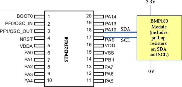
(1) BMP180 pressure/temperature sensor module
(2) NRF905 radio transceiver
(3) STM32F030 MCU

According to the datasheet, the BMP180 has an idle current of 5uA and an active current of up to 650uA. This device is mounted on a breakout board which has a voltage regulator (XC6206) with a quiescent current consumption of 3uA. A MHC5983 magnetometer is also on the board with a quiescent current of 2uA and an active current of 100uA. The total quiescent for this board should be the sum of these : around 10uA. Only the BMP180 is used so the peak current should get to around 650uA.
The NRF905 is powered down when not in use. The datashseet states that its current consumption should get down to 2.5uA when powered down, 32uA when in standby and 20mA when transmitting at +6dBm.
The STM32F030 is put in to deep sleep mode between transmissions. The LSI clock and RTC are left running and periodically wake the system up. It is a little difficult to determine what the current consumption should be in this mode. According to the datasheet, the current consumption should be between 2 and 5 uA. The power consumption of the RTC is of the order of 1uA according to ST literature. During active mode at 8MHz with code executing from flash, the current consumption should be around 4mA.
Adding all of the standby currents up we get to about 10 + 2.5 + 5 + 1 = 18.5uA.
Active mode current flow should be dominated by the STM32F030 and the NRF905. I would expect active mode currents of 5mA with no radio transmission and 25mA during transmission.
The main program loop is as follows:

while(1) {            
    Int2String(readTemperature(),&Msg[0]);    
    Msg[10]=',';
    Int2String(readPressure(),&Msg[11]);       
    TxPacket(Msg,0x20);
    low_power_mode(); // Sleep and wait for RTC interrupt
    resume_from_low_power();        
}

This transmits a packet with the following format:
0000000233,0000099804
This is interpreted as a temperature of 23.3 C and a pressure of 998.04 milibars
The RTC is configured to wake system once per minute (the weather does not change that quickly)
Low power mode is entered and exited with the following two functions:

void low_power_mode()
{					
    PwrLow(); // Put NRF905 into low power mode
    // Turn off GPIO B,A and F		
    RCC_AHBENR &= ~(BIT17+BIT18+BIT22);			
    RCC_APB1ENR &= ~BIT21;   // Turn off clock for I2C1
    RCC_APB2ENR &= ~BIT12;   // turn off SPI1 	
    RCC_CFGR |= 0xf0; // drop bus speed by a factor of 512
    cpu_sleep();      // stop cpu
}
void resume_from_low_power()
{	
    RCC_CFGR &= ~0xf0; // speed up to 8MHz		
    // Turn on GPIO B,A and F
    RCC_AHBENR |= BIT18+BIT17+BIT22;
    RCC_APB1ENR |= BIT21;   // Turn on clock for I2C1
    RCC_APB2ENR |= BIT12;   // turn on SPI1 	
    PwrHigh(); // power up the radio
}

Entering low power mode, the code shuts down the NRF905, disables clocks to the I/O port, I2C and SPI peripherals, slows the peripheral bus clock and stops the CPU. Resuming from low power reverses these steps. The CPU can be placed in shallow or deep sleep modes depending upon the setting of bit 2 in the system control register. The code below enables deep sleep mode which stops the CPU clock and powers down flash memory.

    SCR |= BIT2;  // enable Deep Sleep mode

On receipt of an RTC interrupt, the CPU exits sleep mode and resumes execution.

Results

CurrentConsumption

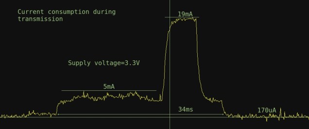
The measured quiescent current was a lot higher than expected; around 170uA @ 3.6V and 90uA at 2.4V. Why is this so much higher? Perhaps passive components on the breakout boards such as pull-down or pull-up resistors are raising the levels. All of the peripherals on the STM32F030 may not be powered off. A current drain of 90uA at 2.4V should allow the station to idle on 1300mAh for more than a year and I felt that this was probably good enough for now. The actual run time is likely to be a lot lower than this due to self discharge in the battery and the energy used during the brief transmission interval. I’ll see how it goes with an extended test.
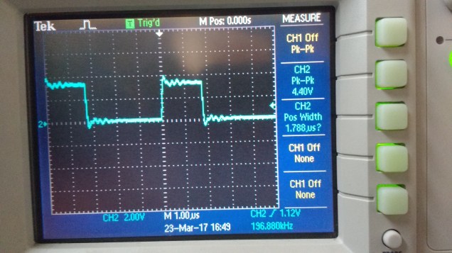
The active mode current is lower than expected. The MCU current just before transmission is about 3mA. It would seem that the radio is only drawing (19-3) = 16mA during transmission. The datasheet suggests that this level of current should be typically 20mA. During experimentation I found that the current levels during transmission were consistently less than suggested by the datasheet – maybe the datasheet typical values are a little overstated.

Looking at the graph, the 5mA (max) region consists of three approx equal length periods: I2C read of temperature, I2C read of pressure and SPI transfer to NRF905. The NRF905 data packet consists of a preamble (10 bits), address (32 bits), data packet (32 bytes) and a CRC field (16 bits). In total this is 538 bits. The data rate if 50kbps which means the transmission time should be 10.76ms. This agrees with the graph.

Debugging issues

I developed this code using my ST-Link V2 debugger salvaged from a Nucleo board and reflashed with J-Link firmware. OpenOCD and GDB allowed me to debug and download code. A problem arises when the CPU is in a deep sleep : OpenOCD can not talk to it in this mode. It complains and times-out repeatedly. Occasionally, it catches the CPU when its awake allowing you halt it and to download code. If the sleep interval is long (e.g. a minute or more) this can be quite frustrating. There is a way around this however. If you pull the Boot0 pin high and power cycle the MCU it will boot to ISP mode. Openocd & GDB can happily attach to this allowing you to download fresh code. When download is complete, set Boot0 to zero and power cycle once more to run your code. You don’t need to stop OpenOCD or GDB when you do this power cycle (I just pulled a wire from the breadboard and put it back again)

Radio range

The NRF905 radio modules were supplied with some short antennas which seemed too short for 433MHz. I found that replacing them with quarter wave length wires slightly improved signal range. I settled on a power output level of 6dBm as it gave me an (urban) range of about 100m – enough for my needs. The radio module seemed to misbehave at the higher power level of +10dBm. This could be as a result of the breakout board or perhaps poor supply regulation. Running it a +6dBm produced stable results.

Code download

You can download the code for the weather station over here on github: https://github.com/fduignan/Weatherstation1

Weather station part 2: The radio link

Introduction

As mentioned in the previous post I’m hoping to put together a weather monitoring system. It will consist of an outstation in the garden which will be solar powered. The outstation will send data over a radio link to a base station located indoors. This post outlines the radio link code and setup.

The outstation radio wiring

stm32f030cct1
The figure above shows the connections between the outstation MCU, the BMP180 pressure/temperature sensor and the NRF905 radio module. There are lots of connections to the radio module and I’m not sure they are all strictly necessary at the moment but for now they stay.
The NRF905 can transmit at a number of different frequencies. After some trial and error I decided to go with a frequency in the 433 ISM band as it seemed to work best (the NRF905 is on a breakout board which already has inductors and capacitors in the antenna circuit which I suspect were tuned for this band). The actual module is supplied from dx.com (link). Overall I found this module much easier to use than the NRF24L01.
The code for the radio link is available on github over here. This code transmits an counter value once per second at maximum power (10mW). This current consumption while transmittiing is quite high (about 29mA) but this current burst is pretty short lived. Early indications are that the range is sufficient for my purposes though I may fiddle with the antenna later to see how far it can be pushed.
A (messy) prototype is shown in the photo below
Stm32f030Bmp180NRF905
You may notice the ST-Link debugger salvaged from a Nucleo board attached to the target. This debugger was reflashed with the Segger/J-Link firmware and behaved very well.

The base station

The base station consists of an STM32L011 Nucleo board attached to an NRF905 module. A photo is shown below (wiring details in the code only for the moment)
stm32l011nrf905
The Nucleo outputs any data it receives over its built-in USB/Serial converter. This is displayed on the host PC.
One problem arose with the STM32L011’s SPI interface which is covered in its errata sheet. There is a timing problem with the SPI pins and ST provide a simple fix for this (which I found out about after two days of head scratching :). Code for the base station is available here

Next post

The next post will deal with the issue of power consumption on the outstation. This needs to be kept as low as possible if the solar power cells I salvaged from cheap garden LED lights are to work out.

Weather station part 1: Pressure and temperature

Introduction

I’ve decided to try to put together a solar powered wireless weather station this summer. It will consist of two parts: an outstation comprising of a pressure/temperature sensor attached to an STM32F030 MCU; all powered by a cheap solar panel and a rechargeable battery. The MCU will use an NRF905 radio module to send data back to a base station within the house which will display it on screen. Power consumption in the outstation will have to be kept to a minimum.
The base station will consist of an STM32L011 Nucleo board and an NRF905 module. It will interface to the host PC using the built-in UART.

The pressure/temperature sensor

About a year ago I bought a BMP180+HMC5983 module from dx.com. The BMP180 component is a very sensitive atmospheric pressure and temperature sensor with an I2C interface. The HMC5983 is a digital magnetometer may have a future role to play in the weather station.

The outstation MCU

I have previously posted a description of how to mount the STM32F030 TSSOP-20 MCU on a breadboard friendly breakout board. These MCU’s can be configured to consume very little energy. I had several of these lying around so the seemed the logical choice.

Wiring

stm32f030_bmp180
The image above shows the wiring involved. The bmp180 module has built-in pull-up resistors so its quite simple. The code on the other hand is quite complicated. The BMP180 has a very strange conversion routine that takes the sensor outputs and converts them to pressure (in Pascals) and temperature (in degrees C x 10). The measurement results are output via the UART TX pin on PA9. I connected this to the host PC using a USB/Serial converter.
The code can be found here. It includes a lot of debugging code that was useful during development. This is very much version 0.1 as it does not take power consumption into account in any way. That will be the subject of a future post.

Interrupt driven display driver for the Arduino nano

CircuitPicture

There are a number of 7 segment display available on the Internet. Some of them use 74595 shift registers to control them. These require the display to be refreshed continuously as the LED’s are multiplexed across a number of digital output pins. I bought one from dx.com (link) though I see they are now out of stock. With a bit of fiddling I came up with the following interrupt driven code to drive it.

The PWM system is used to generate a periodic interrupt on digital output 3. Arduino allows you to attach an interrupt to this pin which works even if the pin is a PWM output. This is done in the setup function. The interrupt handler is set to RefreshDisplay.

The RefreshDisplay function copies the contents of the global array DisplayMemory to the 74595 shift registers in the the display module. One digit is written for each interrupt. After 8 interrupts, all digits have been updated and the process starts over.

The main loop calls on the DisplayNumber function whose job is to take a apart the supplied number into each of its individual digits. The digits are converted to 7-segment LED codes which are stored in DisplayMemory.
The display is connected to the ICSP header of an Arduino nano as shown. The clock and data pins are driven by software.

int SCKPin = 13;
int DIOPin = 11;
int RCKPin = 12;
int DisplayMemory[8];
void setup()
{
  pinMode(RCKPin,OUTPUT);
  pinMode(DIOPin,OUTPUT);
  pinMode(SCKPin,OUTPUT);
// Establish periodic interrupt on digital pin 3 so that RefreshDisplay
// is called regularly
  analogWrite(3,100);
  attachInterrupt(1,RefreshDisplay,RISING);
}
long Count=0;
void loop()
{ 
  DisplayNumber(Count++);
}
const char LED_Codes[]={ 0b11000000,0b11111001,0b10100100,0b10110000,0b10011001,0b10010010,0b10000010,0b11111000,0b10000000,0b10010000 };

void DisplayNumber(long Number)
{
  int Digit;
  for (Digit=0;Digit<8;Digit++)
  {
    DisplayDigit(7-Digit,Number % 10);
    Number = Number / 10;
  }
}
void DisplayDigit(int DigitNumber,int Digit)
{
  DisplayMemory[DigitNumber]=LED_Codes[Digit];
}
void RefreshDisplay()
{
  static  int Digit=1;
  static int Index=0;
  SendByte(Digit);
  SendByte(DisplayMemory[Index]);
  digitalWrite(RCKPin,LOW);
  digitalWrite(RCKPin,HIGH);  
  Digit = Digit << 1;  
  Index++;
  if (Index > 7)
  {
    Index = 0;
    Digit = 1;
  }

}
void SendByte(int Byte)
{
  int Bit;
  for (Bit = 0; Bit < 8; Bit++)
  {
    if (Byte & 0x80)
      digitalWrite(DIOPin,HIGH);
    else
      digitalWrite(DIOPin,LOW);
    Byte = Byte << 1;
    digitalWrite(SCKPin,LOW);
    digitalWrite(SCKPin,HIGH);
  }
}

A very low cost STM32F030 dev board

Aliexpress have begun shipping a low cost breakout/development board for the STM32F030. The board can be programmed using ISP and a USB/UART interface as shown below. The boards cost varies but I got mine for 1.58 Euro.
stm32f030board
I had previously worked on some suitable examples which can be found over here.
These examples are built using a Makefile however I have found that the following script is a lot easier to work with (just make sure your PATH environment variable includes the directory where the arm compiler programs and utilities are stored).

arm-none-eabi-gcc -static -mthumb -g -mcpu=cortex-m0 *.c -T linker_script.ld -o main.elf -nostartfiles 
arm-none-eabi-objcopy -g -O binary main.elf main.bin
arm-none-eabi-objcopy -g -O ihex main.elf main.hex

You then program the chip by linking the Boot0 pin and 3v3 with the jumper, hit reset and enter the following:

stm32flash -w main.hex /dev/ttyUSB0

To run your program, move the jumper so that it links Boot0 to GND and hit reset.
The USB/UART interface appeared as /dev/ttyUSB0 on my system, yours may vary (on Windows it will be something like COM3)
stm32flash can be downloaded from a number of sources. On Ubuntu it can be installed with

sudo apt-get install stm32flash

The ARM cross compiler suite can be downloaded from launchpad.net

Aliexpress link to the board.

Interactive SPI

The SPI protocol can be tricky enough to get working especially if you are unsure of the MCU you are using and/or the peripheral.  Logic analyzers can help but can also be expensive.  With the help of the following Energia MSP430G2553 code and a dumb terminal serial application program (on your PC) you can interact live with an SPI peripheral and hopefully come to grips with its operation.

The peripheral can be wired as follows:
LaunchPads-MSP430G2-—-Pins-Maps-13-42

Launchpad                   Peripheral
MOSI------------------------MOSI
MISO------------------------MISO
P1_0------------------------SS (slave select or CE)
GND-------------------------GND
Vcc-------------------------Vcc

Check the peripheral power requirements first and don’t connect a 5V peripheral directly to a 3.3V MSP430

The program presents the user with a simple menu:

Please select from one of the following:
0: SS Low
1: SS High
2: Write byte
3: Read byte

If you choose 0 or 1, SS is raised or lowered as appropriate and the menu recycles. If you choose 2 you see this (I entered the value ‘a9’ (not case sensitive))

Please select from one of the following:
0: SS Low
1: SS High
2: Write byte
3: Read byte
Enter a 2 character hex value: a9
Out : A9
In : 0

If you choose 3 you will see something like this:

Please select from one of the following:
0: SS Low
1: SS High
2: Write byte
3: Read byte
In : 0

The code is shown below. You will probably need to check out which SPI modes and byte ordering suit you. Also, the SPI interface is running at the very low speed of 125kHz. This was deliberate as it reduces the risk of data errors on shaky test leads and may help debugging. You can of course change this. The divider is divided into 16MHz to give an SPI data rate. This is very definitely version 0.1 and changes are likely in the future when I do some real testing.

/*
 * SPI protocol tester using the MSP430G2553 G2 Launchpad
 * This program allows you manage an SPI bus,write and read data
 * using a serial dumb terminal application
 * The program makes use of the Energia Serial and SPI libraries
 * Serial interface : 9600,n,8,1
 * SPI library reference : http://energia.nu/reference/spi/
 * 
 */
#include <SPI.h>

// Will use P1_0 as SS pin as there is a handy LED there on the launchpad
#define SS_Pin  P1_0


int getUserCommand();
int getInteger(String Prompt);
void setup() {
  // put your setup code here, to run once:
  // Default SPI configuration : feel free to change!
  // Set up the SS Pin and make it HIGH initially (low wakes up a slave)
  pinMode(SS_Pin,OUTPUT);  
  digitalWrite(SS_Pin,HIGH);
  SPI.begin();
  SPI.setDataMode(SPI_MODE0); // can choose modes 0,1,2,3
  SPI.setBitOrder(MSBFIRST);  // can be MSBFIRST or LSBFIRST
  SPI.setClockDivider(128);   // assuming a system clock of 16MHz this gives an 
                              // SPI speed of 125kHz - deliberately slow to be more forgiving and
                              // to make signals easier to see with a scope of logic analyser
  // Serial communications to host setup
  Serial.begin(9600);
}
int TXByte,RXByte;
void loop() {
  
  // put your main code here, to run repeatedly: 
  switch (getUserCommand())
  {
    case 0 : {
      // Command 0 : drop SS pin down
      digitalWrite(SS_Pin,LOW);    
      break;
    }
    case 1 : {
      // Command 1 : raise SS pin up
      digitalWrite(SS_Pin,HIGH);
      break;
    }
    case 2 : {
      // Command 2 : send a byte
      TXByte = getInteger("Enter a value to transmit: ");
      RXByte = SPI.transfer(TXByte);
      Serial.print("Out : ");
      Serial.println(TXByte,HEX);
      Serial.print("In : ");
      Serial.println(RXByte,HEX);
      break;
    }
    case 3 : {
      // Command 3 : read a byte (send a dummy byte out)
      RXByte = SPI.transfer(0x00);
      Serial.print("In : ");
      Serial.println(RXByte,HEX);
      break;      
    }
    default : {
      Serial.println("Invalid choice");
    }
  }
  delay(100);
}
int showMenu(String Menu[],int MenuItemCount)
{
  Serial.flush();
  Serial.println("Please select from one of the following:");
  for (int item=0; item < MenuItemCount; item++)
  {
    Serial.print(item);
    Serial.print(": ");
    Serial.println(Menu[item]);
  }
  while(Serial.available()==0);
    
  return Serial.read() - '0'; // assuming a numeric choice is made - convert to decimal from ascii
}

int getUserCommand()
{
  String Menu[4];
  Menu[0]="SS Low";
  Menu[1]="SS High";
  Menu[2]="Write byte";
  Menu[3]="Read byte";
  return showMenu(Menu,4);
  
}
int HexDigitToDecimal(char Digit)
{
  if ( (Digit >= '0') && (Digit <= '9') )
  {
    return Digit - '0';
  }
  Digit = Digit | 32; // enforce lower case
  if ( (Digit >= 'a') && (Digit <= 'f') )
  {
    return Digit - 'a' + 10;
  }
  return 0;
}
int getInteger(String Prompt)
{
  char HexString[3];
  int ReturnValue = 0;
  HexString[2]=0;
  Serial.flush();
  Serial.print("Enter a 2 character hex value: ");
  while(Serial.available()==0);  
  HexString[0]=Serial.read();Serial.print(HexString[0]);
  while(Serial.available()==0);  
  HexString[1]=Serial.read();Serial.println(HexString[1]);
  ReturnValue = HexDigitToDecimal(HexString[0]);
  ReturnValue = ReturnValue << 4;
  ReturnValue += HexDigitToDecimal(HexString[1]);
  return ReturnValue;
}


Let your code do the wiring

SimpleVsComplex

The image above shows two implementations of the same gaming system (ArcadeSlam). The display has a parallel data interface and the left hand version maps this interface to the 8 bits of a single I/O port on the MSP430 MCU.  A simple write to the port data register is sufficient to write a byte to the display.  From a programming perspective this is easy but, as you can see, the wiring is a little complex.

The version on the right makes use of the connections within the breadboard to connect the display data interface to the MSP430.  This greatly simplifies the wiring however it pushes this complexity back into the code.  The wiring looks like this:

Wiring

The display data interface is spread across Ports 1 and 2.  Not only that, the bits are in reverse order.  Reversing bits at run-time represents a performance hit so, a lookup table was generated and the writing of the data bytes goes from this (for the left hand version)


P2OUT = data;

to

P1OUT &=0xc1;
P2OUT &=0xf8;
if (b)
{ // only write out bits if b is non zero to save time
P1OUT |= reverse_bits[ (b >> 3) ] >> 2;
P2OUT |= reverse_bits[ (b & 0x7) ] >> 5;
}

The lookup table reverse_bits was produced using the following python script (only a 5 bit table was necessary)


#!/usr/bin/python
# Output the specified range of numbers with their
# bits reversed as a lookup table suitable for C
print "const uint8_t reverse_bits[]={ \\"
for n in range(32):
print int('{:08b}'.format(n)[::-1], 2),",\\"
print "};"

Performance is not obviously affected by this wiring change and full code can be downloaded over here on github.

More information can also be found on roboslam.com

Low pass filtering using the STML432 Nucleo

This example uses a 4th order Butterworth low pass filter that was designed in GNU Octave.  The sampling rate was set to 200kHz and the cut-off frequency was set to 20kHz.  The filter output at 20kHz is shown below and, as expected, shows an attenuation of 0.7 (approx the square root of 2).

FilterOutput1

Various attempts were made to optimize the performance of the filter.  The execution time was measured by flipping an output bit either side of the filter code.  An oscilloscope trace of this output is below.

FilterTiming1

As can be seen, the execution time is 1.78 microseconds. This is pretty quick given that floating point numbers are being used.  I found that my attempts to manually improve the performance made no significant difference compared to what the compiler’s optimizer could do.  I also found that gcc’s -O2 optimization setting produced a faster filter than -O3.  The filter shuffles data in the input and output delay lines.  This may be considered less  than optimal but, given that the order of the filter is low, it probably would make little difference to use circular buffers (and manage buffer state etc).

Code can be downloaded here on Github and should be easily compiled on Linux/Windows/Mac

Analogue pass-through at 1MHz on the STM32L432 Nucleo board

Update: I previously had measured (incorrectly) a conversion rate of 4MHz – on moving to better instrumentation this proved to be incorrect.  The maximum stable conversion rate comes out just below 2MHz.  This example runs the system at 1MHz.20kHz_at_4MHz

The STM32L432KC Nucleo board is a low cost board (approx €13) in the same form factor as an Arduino Nano.  The onboard CPU is based on an ARM Cortex M4F running at 80MHz.  It features a very fast ADC and 2 DAC output as well as a number of timers, serial interfaces and so on.

I was curious to see how fast the ADC could be read using a timer as a trigger so I put together a simple program that reads an analogue input and writes this value back out to the DAC.  The graph above shows two traces:  the output is green and is overlaid on top of the input (yellow).  The input signal is a 20kHz sine wave (DC shifted to 1.5V).  The system is reading the input signal and updating the output at 1MHz.  An interrupt service routine (ISR) is called at each ADC conversion which consists of the following code:


void ADC_ISR()
{
  // The green LED output is used to measure the execution time of the ISR
  GPIOB_ODR |= BIT3;   // Turn on green led
  ADC1_ISR = BIT3;     // clear ADC interrupt flag
  GPIOB_ODR |= BIT3;   // Toggle green led
  ADCValue = ADC1_DR;  // Read latest value from ADC conversion
  writeDAC(ADCValue);  // Write new output to DAC
  GPIOB_ODR &= ~BIT3;  // Turn off green led
}

The onboard LED is driven high at the beginning of the ISR and low again on exit.  This allows a measurement to be made of CPU usage inside the ISR.  I used an oscilloscope to monitor the behaviour of the LED pin and this is shown in the trace below

1MHzSamplingCPUUsage

As can be seen, the CPU is loaded to around 25%

Source code for this example and others is available over here on Github

Compiling should be pretty straightforward:

(1) Run the build script (batch file) on Linux/Windows/Mac.

(2) Plug the nucleo board in to your computer and it should appear as disk

(3) Copy “main.bin” to this new “disk”

This should program the board and start the program running.


Multi-threading on the Tiva C Launchpad

Threads and processes

A process is a running program. Multitasking operating systems (e.g Linux, Windows etc.) run a number of processes simultaneously. Each process has a global (or static) memory area, a stack and code. Processes in multitasking OS’s are protected from one another using a hardware based memory management unit. A Scheduler allocates CPU time to each process. The simplest scheduler is a “round-robin” scheduler which allows each process run for a short time before switching to the next allowing each process a turn on the CPU.

multitasking

Threads are similar to processes in some ways however they share the same global/static data as well as the same code but have separate stacks.

threads1

Threads can be scheduled just like processes and so appear to operate in parallel – this is multi-threading.

threads2

Context switching

Each process or thread switch involves a context change: the current processor state (all of its register contents) must be saved and the processor state for the next thread or process loaded.  The image below illustrates a context change from Thread 1 to Thread 2

context_change

The context change is triggered by a timer interrupt and the ARM Cortex processors have a special timer aimed at just this role : the SysTick timer. In the following example the SysTick timer is configured to interrupt the CPU every millisecond which triggers a context change.

ARM Cortex M0 Exception handling

The following registers are placed on the interrupted thread stack (Process Stack) automatically following an interrupt (such as SysTick)

Address Contents
SP Prior to interrupt ????????
SP + 0x0000001C xPSR
SP + 0x00000018 PC
SP + 0x00000014 LR
SP + 0x00000010 R12
SP + 0x0000000C R3
SP + 0x00000008 R2
SP + 0x00000004 R1
SP + 0x00000000 R0

Why not save all of the registers? It is too slow (your ISR may not be changing all registers).

Why just these ones? R0-R3 typically are used for argument passing and should always be preserved by ISR’s. R12 is used by some compilers in their inner function call glue. The LR may hold a function return address. PC must be remembered so we know where to go back to and xPSR must be remembered for the flags.

For a full context switch, the remaining registers must be placed on the Process Stack also.

Address Contents
SP Prior to interrupt ????????
SP + 0x0000001C xPSR
SP + 0x00000018 PC
SP + 0x00000014 LR
SP + 0x00000010 R12
SP + 0x0000000C R3
SP + 0x00000008 R2
SP + 0x00000004 R1
SP + 0x00000000 R0
SP – 0x00000004 R11
SP – 0x00000008 R10
SP – 0x0000000C R9
SP – 0x00000010 R8
SP – 0x00000014 R7
SP – 0x00000018 R6
SP – 0x0000001C R5
SP – 0x00000020 R4

It is not possible carry this out in the C language so a little inline assembler is needed here to complete the context change.


// Preserve remaining registers on stack of thread that is being suspended (Thread A)
asm(" cpsid i "); // disable interrupts during thread switch
asm(" MRS R0,PSP "); // get Thread A stack pointer
asm(" SUB R0,#32"); // Make room for the other registers : R4-R11 = 8 x 4 = 32 bytes
asm(" STMIA R0! , { R4-R7 } "); // Can only do a multiple store on registers up to R7
asm(" MOV R4,R8 "); // Copy higher registers to lower ones
asm(" MOV R5,R9 ");
asm(" MOV R6,R10 ");
asm(" MOV R7,R11 ");
asm(" STMIA R0! , { R4-R7 } "); // and repeat the multiple register store
// Locate the Thread Control Block (TCB) for Thread A
asm(" LDR R0,=TCB_Size "); // get the size of each TCB
asm(" LDR R0,[R0] ");
asm(" LDR R1,=ThreadIndex "); // Which one is being used right now?
asm(" LDR R1,[R1] ");
asm(" MUL R1,R0,R1 "); // Calculate offset of Thread A TCB from start of TCB array
asm(" LDR R0,=Threads "); // point to start of TCB array
asm(" ADD R1,R0,R1 "); // add offset to get pointer to Thread A TCB
asm(" MRS R0,PSP "); // get Thread A stack pointer
// Save Thread A's stack pointer (adjusted for new registers being pushed
asm(" SUB R0,#32 "); // Adjust for the other registers : R4-R11 = 8 x 4 = 32 bytes
asm(" STR R0,[R1] "); // Save Thread A Stack pointer to the TCB (first entry = Saved stack pointer)

// Update the ThreadIndex
ThreadIndex++;
if (ThreadIndex >= ThreadCount)
  ThreadIndex = 0;

// Locate the Thread Control Block (TCB) for Thread B
asm(" LDR R0,=TCB_Size "); // get the size of each TCB
asm(" LDR R0,[R0] ");
asm(" LDR R1,=ThreadIndex "); // Which one is being used right now?
asm(" LDR R1,[R1] ");
asm(" MUL R1,R0,R1 "); // Calculate offset of Thread A TCB from start of TCB array
asm(" LDR R0,=Threads "); // point to start of TCB array
asm(" ADD R1,R0,R1 "); // add offset to get pointer to Thread B TCB
asm(" LDR R0,[R1] "); // read saved Thread B Stack pointer
asm(" ADD R0,#16 "); // Skip past saved low registers for the moment
asm(" LDMIA R0!,{R4-R7} "); // read saved registers
asm(" MOV R8,R4 "); // Copy higher registers to lower ones
asm(" MOV R9,R5 ");
asm(" MOV R10,R6 ");
asm(" MOV R11,R7 ");
asm(" LDR R0,[R1] "); // read saved Thread B Stack pointer
asm(" LDMIA R0!,{R4-R7} "); // read saved LOW registers
asm(" LDR R0,[R1] "); // read saved Thread B Stack pointer
asm(" ADD R0,#32 "); // re-adjust saved stack pointer
asm(" MSR PSP,R0 "); // write Thread B stack pointer

Threads are managed using a structure called a Thread Control Block which is defined as follows:


typedef struct {
uint32_t *ThreadStack;
void (*ThreadFn )();
uint32_t Attributes;
} ThreadControlBlock;

Implementation

A demonstrator application with three threads was developed for the Tiva C Launchpad.  Each thread flashes an LED on the board at a different rate.  The trickiest part to get right was the initial launching of the thread switching which involved a little bit of stack fiddling.  Code is available over here on Github