A simple “blinky” for Zephyr OS on the STM32L432KC Nucleo can be written as follows:
#include <stdio.h>
#include <zephyr/kernel.h>
#include <zephyr/device.h>
#include <zephyr/drivers/gpio.h>

// reference for the STRing macros below:
// https://stackoverflow.com/questions/1562074/how-do-i-show-the-value-of-a-define-at-compile-time
#define XSTR(x) STR(x)
#define STR(x) #x

const struct device *gpio = DEVICE_DT_GET(DT_NODELABEL(gpioa));

int main(void)
{
	printf("Board config = %s\n", CONFIG_BOARD_TARGET);
	printf("Label = %s", XSTR(DT_NODELABEL(gpioa)));
	gpio_pin_configure(gpio,0,GPIO_OUTPUT);
	while(1)
	{
		gpio_pin_toggle(gpio,0);
		printf("Node Label = %s\n", XSTR(DT_NODELABEL(gpioa)));
		printf("GPIO is at %p\n",gpio);
		printf("GPIO device name is %s\n",gpio->name);
		printf("GPIO device config is at %p\n",gpio->config);
		printf("GPIO device api is at %p\n",gpio->api);
		k_msleep(1000);
	}
	return 0;
}
Extra printf’s have been added to try to nail down exactly what is going on with Zephyr devices and device trees. Lets begin by looking at the line that creates our gpio pointer.
const struct device *gpio = DEVICE_DT_GET(DT_NODELABEL(gpioa));
What does this mean?
Well: gpio will be a pointer to a device structure somewhere in the program image (read-only/flash area).
The device structure looks a like this (although shortened a little for brevity, see device.h):
struct device {
	/** Name of the device instance */
	const char *name;
	/** Address of device instance config information */
	const void *config;
	/** Address of the API structure exposed by the device instance */
	const void *api;
	/** Address of the common device state */
	struct device_state *state;
	/** Address of the device instance private data */
	void *data;
	/** Device operations */
	struct device_ops ops;
	/** Device flags */
	device_flags_t flags;
	// some more stuff below omitted.
};
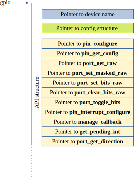
Of greatest significance for this article is the api member of this structure. This is a pointer to a structure that contains the functions we typically use to do GPIO. For GPIO devices this is defined as (gpio.h)
__subsystem struct gpio_driver_api {
	int (*pin_configure)(const struct device *port, gpio_pin_t pin,
			     gpio_flags_t flags);
#ifdef CONFIG_GPIO_GET_CONFIG
	int (*pin_get_config)(const struct device *port, gpio_pin_t pin,
			      gpio_flags_t *flags);
#endif
	int (*port_get_raw)(const struct device *port,
			    gpio_port_value_t *value);
	int (*port_set_masked_raw)(const struct device *port,
				   gpio_port_pins_t mask,
				   gpio_port_value_t value);
	int (*port_set_bits_raw)(const struct device *port,
				 gpio_port_pins_t pins);
	int (*port_clear_bits_raw)(const struct device *port,
				   gpio_port_pins_t pins);
	int (*port_toggle_bits)(const struct device *port,
				gpio_port_pins_t pins);
	int (*pin_interrupt_configure)(const struct device *port,
				       gpio_pin_t pin,
				       enum gpio_int_mode mode,
				       enum gpio_int_trig trig);
	int (*manage_callback)(const struct device *port,
			       struct gpio_callback *cb,
			       bool set);
	uint32_t (*get_pending_int)(const struct device *dev);
#ifdef CONFIG_GPIO_GET_DIRECTION
	int (*port_get_direction)(const struct device *port, gpio_port_pins_t map,
				  gpio_port_pins_t *inputs, gpio_port_pins_t *outputs);
#endif /* CONFIG_GPIO_GET_DIRECTION */
};
So, the gpio pointer variable points to something like this:
How did this happen? How is it used? How does it map to the correct GPIO functions for a specific microcontroller?
Well, like a lot of Zephyr, the answers to all of these questions lie in macros.
The first of these in the above code is: DEVICE_DT_GET(DT_NODELABEL(gpioa)). The inner macro DT_NODELABEL is pretty simple, it just concatenates two symbols together. It is defined in devicetree.h as follows:
#define DT_NODELABEL(label) DT_CAT(DT_N_NODELABEL_, label)
So, the output from this macro in this case should look like this: DT_N_NODELABEL_gpioa
In devicetree_generated.h this is defined as follows:
#define DT_N_NODELABEL_gpioa DT_N_S_soc_S_pin_controller_48000000_S_gpio_48000000
It is this symbol that is passed to the outer macro DEVICE_DT_GET. This in turn causes a further cascade of macro expansions
#define DEVICE_DT_GET(node_id) (&DEVICE_DT_NAME_GET(node_id))
#define DEVICE_DT_NAME_GET(node_id) DEVICE_NAME_GET(Z_DEVICE_DT_DEV_ID(node_id))
#define DEVICE_NAME_GET(dev_id) _CONCAT(__device_, dev_id)
#define Z_DEVICE_DT_DEV_ID(node_id) Z_DEVICE_DT_DEP_ORD(node_id)
#define Z_DEVICE_DT_DEP_ORD(node_id) _CONCAT(dts_ord_, DT_DEP_ORD(node_id))
#define DT_DEP_ORD(node_id) DT_CAT(node_id, _ORD)
#define DT_CAT(a1, a2) a1 ## a2
When all of these macros have been expanded, the result is the address of the device structure for the GPIO Port A. All of this macro evaluation happens at compile time so there is no big run-time overhead.
A Zephyr application will have a number of device structures placed in its flash image. Each follows the broad device structure outlined above. To see how our specific device is handled, lets look at the output from the program:
Node Label = DT_N_S_soc_S_pin_controller_48000000_S_gpio_48000000
GPIO is at 0x80060a4
GPIO device name is gpio@48000000
GPIO device config is at 0x8006470
GPIO device api is at 0x8006374
The first line of this is the symbol name produced by the various macros. This symbol evaluates to the memory address 0x80060a4. If we examine search the linker/compiler map file for this address we get:
0x00000000080060a4 __device_dts_ord_76
This tells us that the index number (ordinal) for the GPIOA device is 76. This is confirmed if we look at the devicetree_generated.hs file in the build/zephyr/include/generated/zephyr/ directory (GPIOA is at address 48000000).
/ *
 * Node dependency ordering (ordinal and path):
 *   0   /
 *   1   /aliases
 *   2   /chosen
 *   3   /connector
 *   4   /soc
 *   5   /soc/interrupt-controller@e000e100
 *   6   /clocks
 *   7   /clocks/clk-hsi
 *   8   /clocks/pll
 *   9   /soc/rcc@40021000
 *   10  /soc/adc@50040000
 *   11  /dietemp
 *   12  /memory@20000000
 *   13  /soc/pin-controller@48000000
 *   14  /soc/pin-controller@48000000/i2c1_scl_pb6
 *   15  /soc/pin-controller@48000000/i2c1_sda_pb7
 *   16  /soc/i2c@40005400
 *   17  /smbus1
 *   18  /soc/i2c@40005c00
 *   19  /smbus3
 *   20  /vbat
 *   21  /vref
 *   22  /clocks/clk-hse
 *   23  /clocks/clk-hsi48
 *   24  /clocks/clk-lse
 *   25  /clocks/clk-lsi
 *   26  /clocks/clk-msi
 *   27  /clocks/pllsai1
 *   28  /cpus
 *   29  /cpus/power-states
 *   30  /cpus/power-states/state0
 *   31  /cpus/power-states/state1
 *   32  /cpus/power-states/state2
 *   33  /cpus/cpu@0
 *   34  /soc/pin-controller@48000000/gpio@48000400
 *   35  /leds
 *   36  /leds/led_0
 *   37  /mcos
 *   38  /mcos/mco1
 *   39  /soc/adc@50040100
 *   40  /soc/pin-controller@48000000/can1_rx_pa11
 *   41  /soc/pin-controller@48000000/can1_tx_pa12
 *   42  /soc/can@40006400
 *   43  /soc/dac@40007400
 *   44  /soc/dma@40020000
 *   45  /soc/interrupt-controller@40010400
 *   46  /soc/rng@50060800
 *   47  /soc/dma@40020400
 *   48  /soc/sai1@40015404
 *   49  /soc/sai1@40015424
 *   50  /soc/pin-controller@48000000/usart2_rx_pa15
 *   51  /soc/pin-controller@48000000/usart2_tx_pa2
 *   52  /soc/rcc@40021000/reset-controller
 *   53  /soc/serial@40004400
 *   54  /soc/serial@40008000
 *   55  /soc/pin-controller@48000000/usart1_rx_pa10
 *   56  /soc/pin-controller@48000000/usart1_tx_pa9
 *   57  /soc/serial@40013800
 *   58  /soc/spi@40003c00
 *   59  /soc/pin-controller@48000000/spi1_miso_pa6
 *   60  /soc/pin-controller@48000000/spi1_mosi_pa7
 *   61  /soc/pin-controller@48000000/spi1_nss_pa4
 *   62  /soc/pin-controller@48000000/spi1_sck_pa5
 *   63  /soc/spi@40013000
 *   64  /soc/spi@a0001000
 *   65  /soc/timer@e000e010
 *   66  /soc/timers@40007c00
 *   67  /soc/timers@40009400
 *   68  /usbphy
 *   69  /soc/usb@40006800
 *   70  /soc/watchdog@40002c00
 *   71  /soc/watchdog@40003000
 *   72  /soc/flash-controller@40022000
 *   73  /soc/flash-controller@40022000/flash@8000000
 *   74  /soc/flash-controller@40022000/flash@8000000/partitions
 *   75  /soc/flash-controller@40022000/flash@8000000/partitions/partition@3c000
 *   76  /soc/pin-controller@48000000/gpio@48000000
 *   77  /soc/pin-controller@48000000/gpio@48000800
 *   78  /soc/pin-controller@48000000/gpio@48001c00
 *   79  /soc/power@40007000
 *   80  /soc/power@40007000/wkup-pin@1
 *   81  /soc/power@40007000/wkup-pin@2
 *   82  /soc/power@40007000/wkup-pin@3
 *   83  /soc/power@40007000/wkup-pin@4
 *   84  /soc/power@40007000/wkup-pin@5
 *   85  /soc/rtc@40002800
 *   86  /soc/rtc@40002800/bbram_regs
 *   87  /soc/timers@40000000
 *   88  /soc/timers@40000000/counter
 *   89  /soc/pin-controller@48000000/tim2_ch1_pa0
 *   90  /soc/timers@40000000/pwm
 *   91  /soc/timers@40000000/qdec
 *   92  /soc/timers@40001000
 *   93  /soc/timers@40001000/counter
 *   94  /soc/timers@40001400
 *   95  /soc/timers@40001400/counter
 *   96  /soc/timers@40012c00
 *   97  /soc/timers@40012c00/counter
 *   98  /soc/timers@40012c00/pwm
 *   99  /soc/timers@40012c00/qdec
 *   100 /soc/timers@40014000
 *   101 /soc/timers@40014000/counter
 *   102 /soc/timers@40014000/pwm
 *   103 /soc/timers@40014400
 *   104 /soc/timers@40014400/counter
 *   105 /soc/timers@40014400/pwm
 */
Our printout shows that the device API is at memory address 0x8006374. Again, if we consult the map file (zephyr.map) we find the following:
app_shmem_regions
                0x0000000008006374        0x0
                0x0000000008006374                __app_shmem_regions_start = .
 *(SORT_BY_NAME(SORT_BY_ALIGNMENT(.app_regions.*)))
                0x0000000008006374                __app_shmem_regions_end = .

k_p4wq_initparam_area
                0x0000000008006374        0x0
                0x0000000008006374                _k_p4wq_initparam_list_start = .
 *(SORT_BY_NAME(SORT_BY_ALIGNMENT(._k_p4wq_initparam.static.*)))
                0x0000000008006374                _k_p4wq_initparam_list_end = .

_static_thread_data_area
                0x0000000008006374        0x0
                0x0000000008006374                __static_thread_data_list_start = .
 *(SORT_BY_NAME(SORT_BY_ALIGNMENT(.__static_thread_data.static.*)))
                0x0000000008006374                __static_thread_data_list_end = .

device_deps     0x0000000008006374        0x0
                0x0000000008006374                __device_deps_start = .
 *(SORT_BY_NAME(SORT_BY_ALIGNMENT(.__device_deps_pass2*)))
                0x0000000008006374                __device_deps_end = .

gpio_driver_api_area
                0x0000000008006374       0x24
                0x0000000008006374                _gpio_driver_api_list_start = .
 *(SORT_BY_NAME(SORT_BY_ALIGNMENT(._gpio_driver_api.static.*)))
 ._gpio_driver_api.static.gpio_stm32_driver_
                0x0000000008006374       0x24 zephyr/drivers/gpio/libdrivers__gpio.a(gpio_stm32.c.obj)
                0x0000000008006398                _gpio_driver_api_list_end = .
This tells us that code from gpio_stm32.c is stored at this address. This code implements an STM32L432 specific version of the Zephyr gpio api. Near the bottom of this file a gpio API structure is constructed as follows:
static DEVICE_API(gpio, gpio_stm32_driver) = {
	.pin_configure = gpio_stm32_config,
#if defined(CONFIG_GPIO_GET_CONFIG) && !defined(CONFIG_SOC_SERIES_STM32F1X)
	.pin_get_config = gpio_stm32_get_config,
#endif /* CONFIG_GPIO_GET_CONFIG */
	.port_get_raw = gpio_stm32_port_get_raw,
	.port_set_masked_raw = gpio_stm32_port_set_masked_raw,
	.port_set_bits_raw = gpio_stm32_port_set_bits_raw,
	.port_clear_bits_raw = gpio_stm32_port_clear_bits_raw,
	.port_toggle_bits = gpio_stm32_port_toggle_bits,
	.pin_interrupt_configure = gpio_stm32_pin_interrupt_configure,
	.manage_callback = gpio_stm32_manage_callback,
};
So, when the program executes the line gpio_pin_toggle(gpio,0); The following code is executed (see gpio.h):
static inline int gpio_pin_toggle(const struct device *port, gpio_pin_t pin)
{
	__unused const struct gpio_driver_config *const cfg =
		(const struct gpio_driver_config *)port->config;

	__ASSERT((cfg->port_pin_mask & (gpio_port_pins_t)BIT(pin)) != 0U,
		 "Unsupported pin");

	return gpio_port_toggle_bits(port, (gpio_port_pins_t)BIT(pin));
}
The last line of this function calls on the stm32l432kc version of port_toggle_bits by first looking up the device structure address, then the address of the api structure within it and finally, the .port_toggle_bits (= gpio_stm32_port_toggle_bits) within it. So, at runtime there is a little extra overhead in the sense that a couple of pointers have to be followed but the upside is that it greatly facilitates the writing of device independent code.